—Knowing and doing are the farthest distances in the world.
In previous articles, we introduced the aspects that need to be considered in the front-end architecture and design of SoC, and provided some reference solutions. The last article described the relevant content of UPF, completing the overall plan and UPF. The next step is the physical implementation. During the physical implementation process, how do we consider low power consumption? I have not actually worked on the back-end, and my experience is mostly theoretical. Here, I can only attempt to provide some reference answers, and I welcome corrections from experienced back-end engineers passing by.
Brief Process of Physical Implementation
The physical implementation is the process of converting the design files completed in the front-end, RTL/SDC/UPF, into GDS. The basic process of back-end physical implementation is shown in the figure below.

Logic synthesis: Read in the design files RTL/SDC/UPF and related library files, converting the logical design into a gate-level netlist.
FloorPlan: Set the physical dimensions, shapes, and placements of Memory, Macro, Port, etc.
Layout: Also known as Place, automatically perform stdcell layout, timing, power consumption, and area optimization using tools.
CTS: Clock Tree Synthesis, combines FloorPlan and layout to construct the clock tree. The clock before CTS is ideal (clock path delay is 0)
Routing: Route to achieve the physical connections of all cell nets. After completion, power consumption, area, and timing optimizations will be performed, excluding power, analog, etc.
Timing convergence: Timing convergence with real delays from library files.
Physical rule check: Quality checks during the implementation of the above steps, fixing issues that cannot be resolved by repair tools.
Types of Physical Standard Cells
Flip-Flop Cell
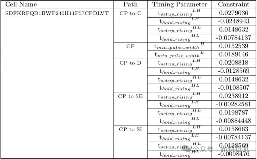
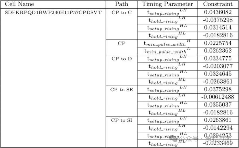
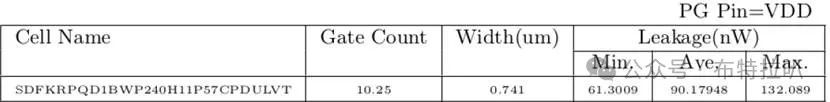
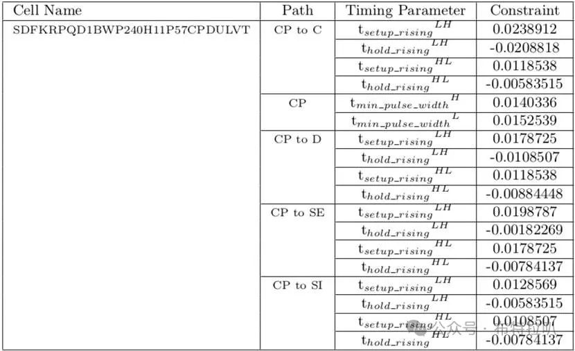
From TSMC DataSheet, a type of SDF is shown below.
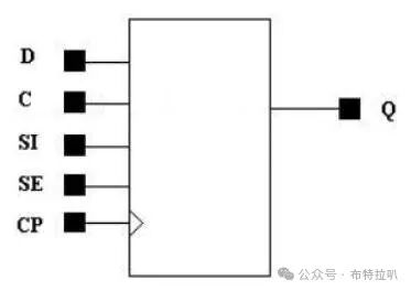
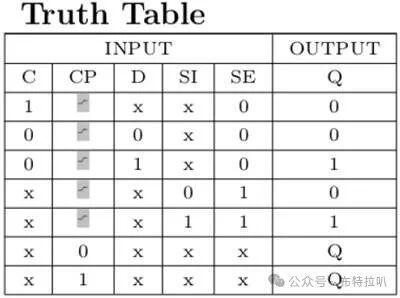
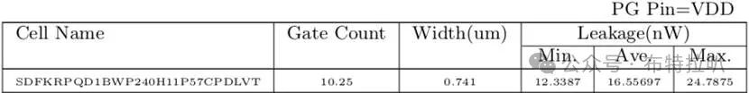
Different types of standard cells have different characteristics; some have low power consumption, while others have good performance. The selection needs to be balanced. Below are the characteristics of different DFF cell types as shown in the figure above (data source: TSMC process library files, Corner is the same, TT0P85V85C).
LVT:
SVT:
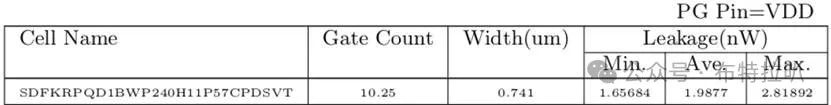
ULVT:
|
Cell Type |
Gate Count |
Leakage(Avg,nW) |
Timing (CP to D,ns) |
|
LVT |
10.25 |
16.55697 |
Setup LH: 0.021 Hold LH: -0.013 |
|
SVT |
10.25 |
1.9877 |
Setup LH: 0.033 Hold LH: -0.020 |
|
ULVT |
10.25 |
90.17948 |
Setup LH: 0.018 Hold LH: -0.010 |
The comparison results of the three types of Cell are as follows:
l Area, Gate Count is the same.
l Power consumption, SVT is the minimum, followed by LVT, and ULVT is the maximum.
l Timing, ULVT is the minimum, followed by LVT, and SVT is the maximum.
If only low power consumption is considered, the preferred type is SVT type Cell. However, a balance must be struck between performance and power consumption, aiming to choose cells with low power consumption while meeting performance requirements to achieve overall power savings.
Unresolved Issues: How can the three types of Cell with the same Gate Count achieve the same functionality while having such significant differences in leakage/timing?
Multibit Cell
Next, let’s look at the Multibit Cell, which is widely used for both reducing power consumption and minimizing area. Its characteristic is that a single Cell contains multiple bits of logic. I understand that each individual Cell has the same logic, such as SI/SE/CP. When they are dispersed, due to layout and routing, there will inevitably be repetitions. If we merge them together, similar logic can be reused as much as possible, achieving the goal of reducing power consumption and area. Depending on the number of bits merged, there are 2bit MB, 4bit MB, 6bit MB, and 8bit MB.
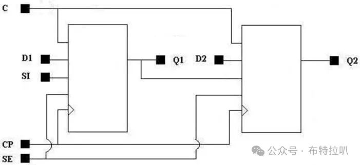
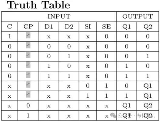
Below is a structural diagram and truth table for the 2bit MB LVT Cell:
Its PPA data is as follows:
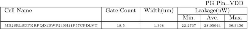
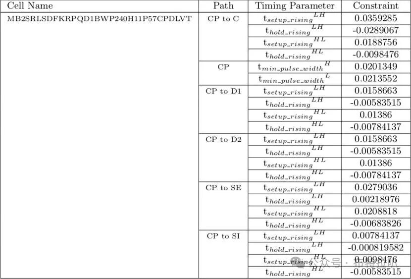
The comparison between the 2bit MB LVT cell and two 1 bit LVT cells is as follows:
|
Cell Type |
Gate Count |
Leakage(Avg,nW) |
Timing (CP to D,ns) |
|
2MB |
18.5 |
28.05 |
Setup LH: 0.015 Hold LH: -0.006 |
|
1 B * 2 |
10.25 *2 = 20.5 |
16.55697 * 2 ≈33.2 |
Setup LH: 0.021 Hold LH: -0.013 |
From the above data, the 2bit MB cell is better optimized in area, power consumption, and timing compared to two 1bit cells. The same applies to 4bit MB, 6bit MB, and 8bit MB, which will not be listed one by one. Overall, under the premise of meeting performance requirements, we should use as many MB cells as possible in conjunction with the actual layout and routing of PD to achieve the goals of reducing area and saving power consumption.
Memory Cell
In addition to the standard Cell, another part is Memory. The selection of memory also requires balancing. Besides the choice of the memory itself, the stitching form of large-capacity memory is also a science. The table below shows four different stitching methods to create the same storage capacity. The first column is the stitching method number, the second column is the selected memory module, the third column is the area data of the memory module, the fourth column is the power consumption under different modes, the fifth column is the number of chips required for stitching, and the sixth column is the overall area and power consumption data.
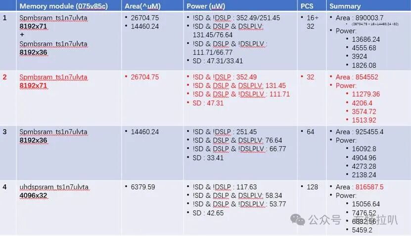
From the table, it can be seen that without considering routing, the fourth method has the smallest area, while the second method has the lowest power consumption. However, the fourth method requires 128 chips, which will lead to more routing space between individual memory chips. Therefore, the second method is selected as the optimal choice.
IR Drop
During physical implementation, an important issue to consider is IR Drop. IR Drop refers to the voltage drop that occurs during voltage transmission due to the resistance of the routing or noise in the ground plane. If the drop is significant, the corresponding delay of the STD Cell will also be affected, impacting the chip’s functionality. For high-performance designs, IR Drop needs to be controlled within a very small range.IR drop is mainly divided into two types: static IR drop and dynamic IR drop.
Static IR Drop: The cause is the resistance of the power network metal connections, which causes a portion of the voltage to drop when current flows through. Therefore, static IR drop is mainly related to the structure and routing details of the power network. Thus, static IR drop mainly considers the resistance effect. When satisfying physical design rules, efforts should be made to reduce resistance values, such as adjusting line widths and optimizing routing lengths. The overall length actually goes from the external power output to the final std cell, passing through PCB routing, packaging, power networks, and other long paths, all of which need to be considered.
Dynamic IR Drop: The cause is the voltage drop caused by current fluctuations during circuit switching. This phenomenon occurs at the clock’s trigger edge, where the clock edge transition not only brings a large number of transistor switches but also causes transitions in combinational logic circuits, often generating a large current across the entire chip in a short time. This momentary large current causes the IR drop phenomenon. The more transistors that switch, the more likely it is to trigger dynamic IR drop phenomena.
Since the occurrence of IR Drop is unavoidable, how should we solve this problem? Common methods include:
l Optimize the power network, such as power planes, ground plane divisions, metal routing widths, spacings, etc.
l Increase power vias to reduce mutual influence between different power sources.
l Add decoupling capacitors. The characteristic of capacitors is that they behave as open circuits for DC power and form impedance for AC power. When there is instantaneous current, the capacitor will form impedance to hinder the change of instantaneous current, reducing the amplitude of the voltage drop.
l When the density of local std cells is too high, try to disperse the layout, which is also significantly related to the front-end code.
l If the number of power sources is too small, causing one power source to drive too many loads, it will also create voltage drops. Increase the number of power sources.
l Use low-resistance materials for metal routing.
Summary
This article attempts to explain the power design considerations related to physical implementation, including the selection of STD Cell types, Memory selection and stitching schemes, IR Drop, etc. It is sufficient to have a general understanding without delving into back-end details. Thus, the introduction to the architecture principles and design implementation of the power consumption series is basically complete. After completing the architectural design and implementation, how do we ensure that the design meets expectations? The answer is verification, including:
1.The architectural power design intent needs to carry UPF for front-end NLP simulation.
2.RTL implementation of low power methods, normal DV verification, power analysis optimization design methods. Power analysis is divided into two types: in the early stage, establish a power analysis model to simulate the operation of IP to guide the design of IP, and in the later stage, analyze the design within IP to find optimization space.
3.UPF syntax quality itself, completing VLCP checks.
4.DRC Check after the implementation of PD.
These parts will not be explained for now, leaving it as a work in progress.