SoC and Chiplet Integration1. Introduction
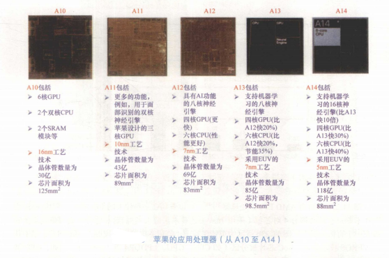
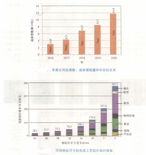
SoC integrates ICs with different functions into a single chip for a system or subsystem. The figure shows the evolution of Apple’s application processors (AP) from A10 to A14, illustrating the relationship between the number of transistors in chips of different feature sizes and the years. It is evident that the number and functionality of transistors in chips increase as feature sizes decrease. Unfortunately, according to research by International Business Strategies, the figure shows the relationship between the design costs of advanced process chips and decreasing feature sizes (down to 5nm). It can be seen that designing a chip with a 5nm feature size alone requires over $500 million, and the development of 5nm process technology requires an additional $1 billion.
2.Chiplet Heterogeneous Integration vs. SoC
Chiplet heterogeneous integration differs from SoC. Chiplet heterogeneous integration redesigns SoCs into smaller chiplets, then utilizes packaging technology to integrate chiplets made from different materials, with different functions, designed by different companies and foundries, and with varying wafer sizes and feature sizes into a single system or subsystem. One chiplet is a functional integrated circuit (IC) module composed of reusable IP (Intellectual Property) blocks.
3.Different Methods of Chiplet Heterogeneous Integration
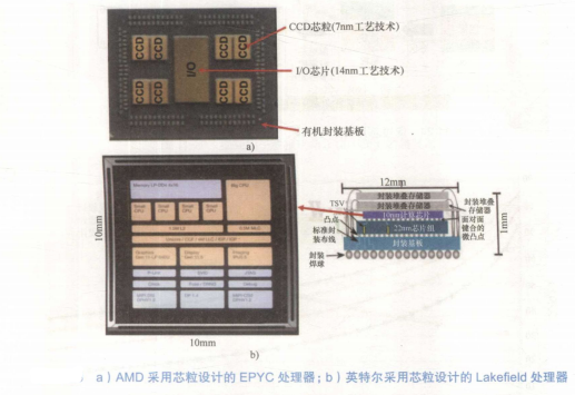
Figure a shows the AMD EPYC processor. It can be seen that there are four pairs of chiplets (manufactured using 7nm process technology) tightly mounted on an organic substrate, flanking a larger I/O chip (manufactured using 14nm process technology) through bonding and bottom filling. Figure b shows Intel’s mobile (laptop) processor “Lakefield,” manufactured based on its FOVEROS technology. The SoC chip is partitioned (e.g., CPU, GPU, LPDDR4, etc.) and split (for example, the CPU is split into a large CPU and four small CPUs) into chiplets, which are then face-to-face bonded (stacked) onto an active TSV interposer (a large 22FFL base chip) using CoW technology.
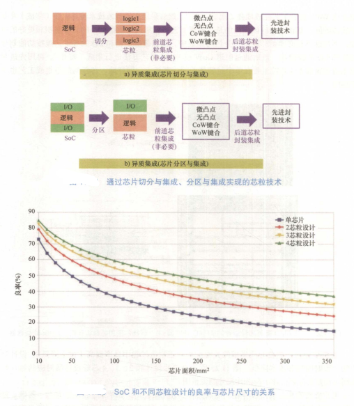
As shown in the figure, there are currently at least two different methods of chiplet heterogeneous integration: chip splitting and integration (driven by cost and yield) and chip partitioning and integration (driven by cost and technology optimization). In chip splitting and integration, logic chips such as SoCs are split into smaller chiplets, such as logic1, logic2, and logic3. These chiplets can be stacked (integrated) through front-end CoW bonding or WoW bonding processes, and then assembled (integrated) using advanced packaging technology on the same substrate of a single package.
It should be emphasized that front-end process chiplet integration can achieve smaller package areas and better electrical performance, although this is not mandatory. In chip partitioning and integration, for example, an SoC with logic and I/O is functionally divided into logic and I/O chiplet modules, which are then integrated (stacked) using front-end CoW or WoW process methods. Advanced packaging technology is then used to assemble the logic and I/O chiplets on the same substrate of a single package. Similarly, the front-end integration process of chiplets is also not mandatory.
4.Key Advantages of Chiplet Heterogeneous Integration
Compared to SoC, the key advantages of chiplet heterogeneous integration include improved yield during the manufacturing process (lower costs), shorter time-to-market during the design process, and reduced costs. The figure shows the relationship between the yield (percentage of good chips) of single-chip designs and 2, 3, and 4 chiplet designs with chip size. Process scaling of SoCs will continue to exist. However, only a few companies, such as Apple, Samsung, Huawei, and Google, can afford smaller feature sizes (advanced process nodes). Typically, they adopt this approach for several reasons; for example, Apple has at least three reasons:
1) Since Apple acquired Palo Alto Semiconductor on April 23, 2008, it has been building chips with a large amount of IP and tightly coupling (integrating) them with its software development.
2) The additional interconnect and communication overhead between chips brings more issues, making it less attractive to decompose its SoC design into chiplets.
3) The world’s leading foundry (TSMC) is a loyal partner of Apple, committed to completing Apple’s products, for example, the application processor (A16) is planned to be manufactured using TSMC’s 3nm process technology in the second half of 2022.
ENDFor more inquiries, please followWeChat public account:Chip Manufacturing and PackagingLikeShareFavorite