In a previous article, we briefly analyzed the architecture of MCU chips.Analysis of MCU chip system architectureIn fact, most WIFI chips can be considered as MCU chips, so the SoC architecture of WIFI chips is basically the same as that of MCU chips, which includes the CPU, bus, peripherals, and of course, the WIFI IP itself.Below, we will briefly analyze how to build a WIFI chip SoC system, taking the ESP32-S3 specifications as an example (the following is only my personal analysis process and is not related to the actual S3 chip architecture).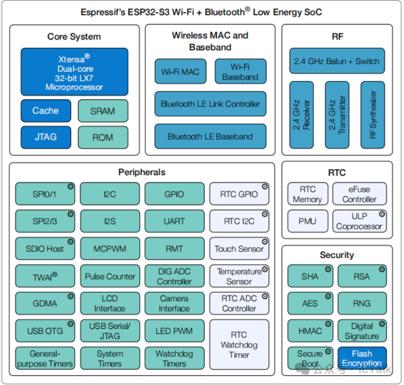
- Determine the system’s bus architecture
The bus architecture of the system is the core of the entire chip. To determine the system’s bus architecture, we need to consider several aspects, including the CPU architecture, bus master/slave division, and master/slave interconnection network.
- CPU architecture:
Based on the CPU’s clock frequency, the number of CPU cores, the number of CPU master interfaces, whether each master needs to support cache, the required SRAM and ROM sizes, and whether TCM support is needed, we can roughly determine the CPU system’s bus architecture.For example, in the case of the S3, according to the specifications, it has two CPUs, which support IBUS and DBUS. The data width of the IBUS is 32 bits, while the DBUS can reach a data width of 128 bits, supporting 384KB ROM, 512KB SRAM, and 16KB RTC memory. It also requires cache access to external memory, so we can determine a basic CPU architecture.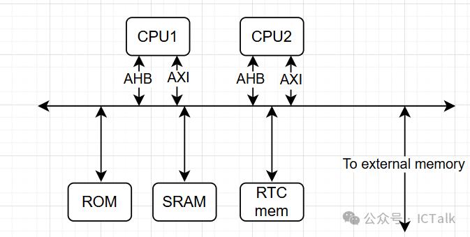 Since the data width of the DBUS can be 128 bits, it is likely an AXI interface. As for whether the interfaces of various memories are AXI or AHB, it can theoretically be either, and should be analyzed based on the specific situation.
- Bus master/slave division
Determine which are bus masters and which are bus slaves based on actual application scenarios. For the S3, the WIFI system is definitely a master, and other masters include SDIO, USB, DMA, security IP, etc., while the rest are basically slave interfaces.For slave interfaces, we can further distinguish between high-speed and low-speed slaves. Typically, high-speed slaves can use AXI or AHB interfaces, while low-speed ones can use APB interfaces. However, this is not absolute; many IP register configuration ports can also be AHB interfaces, depending on the actual situation.After determining all masters and slaves, we can outline the bus structure.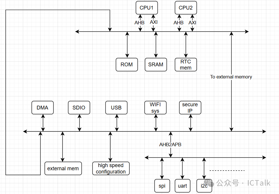
- Master/slave interconnection network
Based on the actual usage scenarios, determine which master needs to access which slave in the bus structure to generate a complete bus matrix mesh network.For example, for an SDIO device, it usually does not need to access AHB2APB slaves, while USB needs to access SRAM, and DMA typically needs to access both SRAM and peripherals, etc.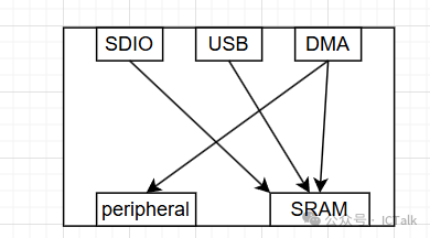 Additionally, when determining the bus architecture, an important metric to evaluate is the throughput of each master/slave. For example, SDIO 3.0 UHS-I can achieve a maximum throughput of 104MB/s. Assuming the frequency of the SDIO AHB master is 20MHz (which is generally not this low), the throughput of the master interface would be 80MB/s, which is lower than the throughput of the SDIO interface itself, clearly not meeting the requirements. For higher-speed interfaces like PCIe, a comprehensive evaluation is needed to determine whether to use AHB or AXI for the master and what data width will meet the throughput requirements of the PCIe interface.
- Power domain division
The division of power domains is also crucial for an SoC system, as power saving is an eternal theme. Based on actual usage scenarios, reasonable division of power domains can achieve optimal power consumption. The S3 has three low-power modes.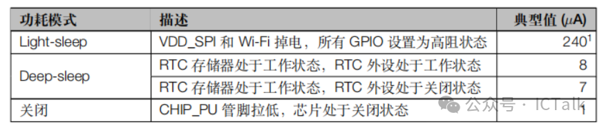 For example, in the light-sleep mode, the CPU stops running, while the MAC/host/RTC/external interrupts can wake the chip. The PHY+RF module can power down but maintain a connection with the AP.This shows that PHY+RF can be a power domain, while the MAC’s TBTT interrupt/RTC/external interrupts also need to be in a non-power-down power domain, and the CPU can be in a retention state, etc.
- Determine IOMUX
The need for IOMUX arises because the pins on the chip are never enough. It is necessary to multiplex various functions to different pins more conveniently, providing customers with more options. Therefore, determining the IOMUX scheme is also very important. It is essential to consider various usage scenarios, which functions will be used simultaneously, and which will definitely not be used simultaneously, ultimately determining which functions can be multiplexed to the same pin. Some of the multiplexing functions of the S3 are as follows.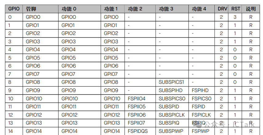 At this point, an initial SoC architecture can be constructed, and the subsequent steps involve optimizing various details, such as considering clock, reset, DFT design, boot, test modes, etc.The end!