 Source: Semiconductor Materials and Process EquipmentOriginal Author: XKX
Silicon Carbide Technology: A Key Force Leading Innovation in the Semiconductor Field
Silicon Carbide (SiC) is an advanced semiconductor material that offers tremendous potential for breakthrough developments in semiconductor technology. This article will comprehensively explore the significance, key technologies, and application prospects of silicon carbide technology in the semiconductor field, covering its origins, structural properties, epitaxial growth, wafer manufacturing, device design, packaging, and modularization.Silicon carbide (SiC) is an important semiconductor material with a wide range of applications. Its origins can be traced back hundreds of years when people began to study and utilize certain ores.As early as ancient times, people recognized the properties and uses of specific ores. One such ore, known as “Moissanite,” caught people’s attention. In 1891, French chemist Henri Moissan discovered a very rare crystal in a volcanic eruption’s meteorite, which was later named “Moissanite.” Moissan classified this substance as silicon carbide and conducted in-depth studies on its properties.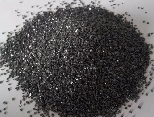 However, it was not until the mid-20th century that the preparation and application of silicon carbide began to develop significantly. In the 1940s, American scientist Edward Goodrich Acheson invented a method known as the “Acheson process,” which involved heating graphite and silica in an electric furnace at high temperatures to produce synthetic silicon carbide through carbothermal reduction. This discovery marked the beginning of silicon carbide’s recognition as an independent material in the scientific community.In the following decades, silicon carbide gradually found applications in various fields. In the semiconductor sector, due to its excellent physical and chemical properties, such as high melting point, high electron mobility, high thermal resistance, and lower energy bandgap, it has been extensively researched as an alternative to silicon. The wide bandgap of silicon carbide allows it to operate in high-temperature and high-voltage environments, which is crucial for high-power applications and high-temperature electronic devices. Additionally, silicon carbide exhibits lower electron drift rates, higher breakdown field strength, and higher thermal conductivity, making it widely used in power electronics, optoelectronics, and wireless communications.The structure and properties of silicon carbide (SiC) significantly influence its applications. SiC crystals possess various crystal structures, with the most common being 4H-SiC and 6H-SiC. These structures consist of a crystal lattice made up of silicon (Si) and carbon (C) atoms.The basic structure of SiC crystals is formed by alternating layers of silicon and carbon atoms. This arrangement creates a hexagonal lattice structure, similar to that of graphite, but with a different arrangement of silicon and carbon atoms. In the 4H-SiC and 6H-SiC structures, silicon atoms form a three-dimensional structure, while carbon atoms form hexagonal layers.Characteristics of SiC crystals include:Wide Bandgap: SiC crystals have a larger bandgap than silicon, allowing SiC to operate in high-temperature and high-voltage environments. The wide bandgap results in lower electron and hole concentrations, reducing the recombination rate of charge carriers and enhancing the device’s operating speed and efficiency.High Melting Point and Thermal Stability: SiC has a high melting point (approximately 2700°C), providing good stability in high-temperature environments. This allows SiC devices to operate in high-temperature applications without the need for additional cooling systems.High Electron Mobility: SiC has a high electron mobility, which refers to the speed at which electrons move through the material. High electron mobility enables SiC devices to achieve high-speed operation and high-frequency applications.High Breakdown Field Strength: SiC has a high breakdown field strength, which is the maximum electric field strength the material can withstand. High breakdown field strength allows SiC devices to operate in high-voltage applications while reducing size and weight.Lower Electron Drift Rate: Despite having high electron mobility, SiC also exhibits a lower electron drift rate. This means that electrons move more slowly under the influence of an electric field, reducing the flow speed of current. This is beneficial for certain applications, such as power devices.High Thermal Conductivity: SiC has high thermal conductivity, enabling SiC devices to quickly dissipate generated heat, improving the thermal stability of the devices.
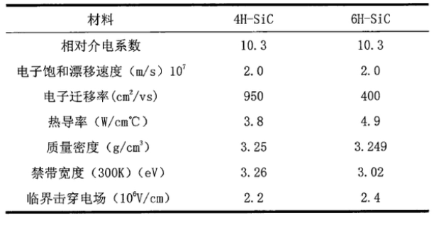 Silicon Carbide Epitaxy: Pioneering New Frontiers in the Semiconductor FieldSilicon carbide (SiC) epitaxy is an advanced semiconductor fabrication technology that has brought significant breakthroughs to the electronics industry. This article will introduce the basic concepts of silicon carbide epitaxy, its application fields, and its importance in the semiconductor sector.What is Silicon Carbide Epitaxy? Silicon carbide epitaxy is a semiconductor material fabrication technology used to grow high-quality silicon carbide films on substrates. It involves placing the substrate in a reaction chamber and depositing silicon carbide material layer by layer on the substrate surface using methods such as Chemical Vapor Deposition (CVD) or Physical Vapor Deposition (PVD).Application Fields of Silicon Carbide Epitaxy:Power Electronic Devices: Silicon carbide epitaxy technology provides feasible solutions for the fabrication of power electronic devices (such as power MOSFETs, Schottky diodes, etc.). Due to the excellent characteristics of silicon carbide, such as high breakdown field strength, high electron mobility, and low leakage current, silicon carbide materials grown through epitaxy can achieve high efficiency and high-temperature operation.Optoelectronic Devices: Silicon carbide epitaxy technology also provides an important foundation for the fabrication of optoelectronic devices. Silicon carbide materials have high refractive indices and wide-band response characteristics, making them widely used in optical communications, laser diodes, and optical sensors.Radio Frequency (RF) Devices: Silicon carbide epitaxy technology has potential applications in the manufacturing of RF devices. Silicon carbide materials possess low loss, high electron mobility, and high thermal conductivity, making them ideal for RF power amplifiers, high-frequency switches, and wireless communication devices.Advantages of Silicon Carbide Epitaxy:High-Quality Materials: Silicon carbide epitaxy technology can grow high-quality, lattice-matched silicon carbide films on substrates, ensuring the reliability and consistency of the materials.Customized Growth: Epitaxy technology allows for customized growth based on specific requirements, including control over thickness, doping, and crystal orientation to meet the needs of different applications.Resource Savings: Compared to other fabrication methods, silicon carbide epitaxy technology has higher material utilization rates and lower material waste, conserving resources and improving production efficiency.Silicon Carbide Substrates: Achieving Breakthrough Developments in Semiconductor DevicesSilicon carbide (SiC) substrates are a key semiconductor material that provides a reliable foundation for the fabrication of silicon carbide devices. This article will delve into the characteristics, fabrication methods, and importance of silicon carbide substrates in various application fields.Characteristics of Silicon Carbide Substrates: Silicon carbide substrates possess several unique characteristics that make them ideal for semiconductor device fabrication.Wide Bandgap: Silicon carbide substrates have a larger bandgap than silicon, making them suitable for high-temperature, high-power, and high-frequency applications. The wide bandgap reduces the recombination rate of charge carriers, enhancing the efficiency and reliability of devices.High Thermal Stability: Silicon carbide substrates can operate stably in high-temperature environments, exhibiting excellent thermal stability and thermal conductivity. This allows silicon carbide devices to withstand high power and temperature operations, reducing heat accumulation and thermal stress.High Breakdown Field Strength: Silicon carbide substrates have high breakdown field strength, making them perform excellently in high-voltage applications. This allows silicon carbide devices to reduce size and weight while increasing power density.Excellent Carrier Mobility: Silicon carbide substrates have high electron and hole mobilities, enabling devices to perform excellently in high-frequency operations and high-speed switching applications.Fabrication Methods of Silicon Carbide Substrates:The fabrication methods of silicon carbide substrates mainly include the following two:Physical Vapor Deposition (PVD): This method involves depositing silicon carbide on the substrate surface at high temperatures using techniques such as thermal evaporation, electron beam evaporation, and magnetron sputtering.
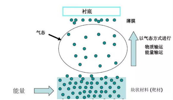 Chemical Vapor Deposition (CVD): This method involves chemically reacting precursor gases on the substrate surface at high temperatures to deposit silicon carbide, including Low-Pressure Chemical Vapor Deposition (LPCVD) and Gas-Source Epitaxy (GSE).
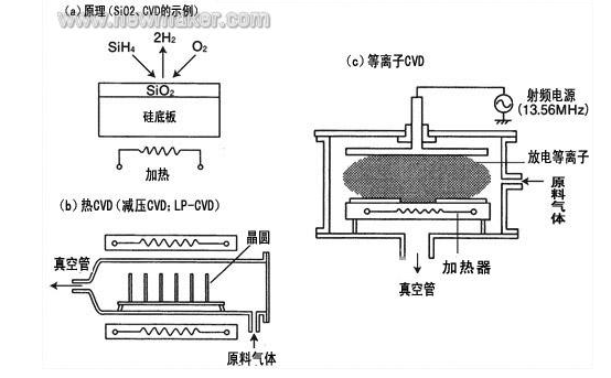 These methods can control the growth rate, lattice matching, and surface quality of silicon carbide substrates, ensuring high-quality silicon carbide substrates are obtained.Application Fields of Silicon Carbide Substrates:Silicon carbide substrates have wide applications in multiple fields:Power Electronic Devices: Silicon carbide substrates are widely used in high-power electronic devices such as power MOSFETs, Schottky diodes, and power modules. Their excellent performance allows these devices to operate stably in high-temperature and high-voltage environments.Optoelectronic Devices: Silicon carbide substrates play an important role in optoelectronic devices, such as photodetectors, laser diodes, and optoelectronic sensors. Their wide-band response and high thermal stability make them ideal for high-performance optoelectronic devices.Radio Frequency (RF) Devices: Silicon carbide substrates have potential in RF devices, such as RF power amplifiers, high-frequency switches, and wireless communication devices. Their high thermal stability and high breakdown field strength make them suitable for high-power and high-frequency RF applications.Silicon Carbide Device Design: Achieving Breakthroughs in Performance and EfficiencySilicon carbide (SiC) device design is a crucial step in achieving breakthroughs in semiconductor technology. This article will explore the principles, key characteristics, and importance of silicon carbide device design in various application fields.Principles of Silicon Carbide Device Design:Silicon carbide device design aims to fully utilize the characteristics of silicon carbide materials, such as wide bandgap, high thermal stability, high breakdown field strength, and high electron mobility. Based on these characteristics, silicon carbide device design focuses on the following aspects:Structural Optimization: By optimizing device structure and layout, the resistance, capacitance, and inductance parameters can be minimized to achieve high performance and efficiency.Electric Field Control: By designing electric field distribution and gradients, the breakdown field strength can be maximized, reducing resistance and leakage current to achieve high power density and efficiency.Temperature Management: Considering the stability and heat dissipation of devices in high-temperature environments, optimizing heat dissipation structures and material selection can achieve high-temperature operation and long lifespan.Key Characteristics of Silicon Carbide Device Design:High Electron Mobility: Silicon carbide has high electron mobility, enabling devices to achieve high-speed operation and high-frequency applications.Wide Bandgap: The wide bandgap of silicon carbide allows it to operate in high-temperature and high-voltage environments, suitable for high-power and high-temperature applications.High Thermal Stability: Silicon carbide exhibits excellent thermal stability, allowing stable operation in high-temperature environments, suitable for high power density and high-temperature applications.High Breakdown Field Strength: Silicon carbide has high breakdown field strength, enabling devices to withstand high-voltage operations, reducing size and weight.Importance of Silicon Carbide Device Design in Different Application Fields:Power Electronics: Silicon carbide device design is crucial for high-power electronic devices such as power MOSFETs, Schottky diodes, and power modules. Through reasonable device design, high efficiency, high frequency, and high-temperature operation can be achieved.Optoelectronics: Silicon carbide device design holds significant importance in optoelectronic devices such as photodetectors, laser diodes, and optoelectronic sensors. Proper device design can enhance the performance and efficiency of optoelectronic devices.Radio Frequency (RF): Silicon carbide device design has potential in RF power amplifiers, high-frequency switches, and wireless communication devices. Optimized device design can achieve high speed, high frequency, and high efficiency in RF applications.Silicon Carbide Wafer Manufacturing: The Key to High-Quality and Large-Scale ProductionSilicon carbide (SiC) wafer manufacturing is a critical step in achieving large-scale production of silicon carbide devices. This article will explore the process flow, key technologies, and importance of silicon carbide wafer manufacturing in the semiconductor industry.Process Flow of Silicon Carbide Wafer Manufacturing:Substrate Selection: Selecting suitable single-crystal silicon carbide substrates as the starting material for growth, typically using methods such as Chemical Vapor Deposition (CVD) or Physical Vapor Deposition (PVD).Material Growth: Using epitaxy technology, silicon carbide material is grown layer by layer on the substrate surface, controlling growth conditions and crystal structure to obtain high-quality silicon carbide wafers.Material Processing: After growth, silicon carbide wafers undergo Chemical Mechanical Polishing (CMP) and oxidation treatments to achieve a smooth surface and good interface quality.Control and Inspection: Through surface inspection, crystal structure analysis, and electrical testing, strict quality control is performed on silicon carbide wafers to ensure compliance with required electrical characteristics and crystal quality.
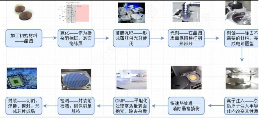 Key Technologies in Silicon Carbide Wafer Manufacturing:Epitaxy Technology: Epitaxy technology is the core of growing high-quality silicon carbide wafers. By using Chemical Vapor Deposition (CVD) or Physical Vapor Deposition (PVD) methods, growth conditions and crystal structures are controlled to achieve high-quality silicon carbide wafer growth.Wafer Processing Technology: This includes mechanical polishing, Chemical Mechanical Polishing (CMP), and wafer slicing processes to achieve smooth surfaces and accurate wafer dimensions.Quality Control Technology: Through surface inspection, X-ray diffraction, and electrical testing, strict quality control is performed on silicon carbide wafers to ensure compliance with required electrical characteristics and crystal quality.Importance of Silicon Carbide Wafer Manufacturing in the Semiconductor Industry:Achieving Large-Scale Production: High-quality silicon carbide wafer manufacturing is a crucial step in achieving large-scale production of silicon carbide devices. High-quality silicon carbide wafers can meet the semiconductor industry’s demand for high-performance and high-reliability devices.Promoting the Development of Silicon Carbide Technology: Improvements in silicon carbide wafer manufacturing promote the development and application of silicon carbide technology, facilitating the widespread use of silicon carbide devices in power electronics, optoelectronics, and RF fields.Improving Production Efficiency: Continuous advancements in silicon carbide wafer manufacturing technology enhance the production efficiency and yield of silicon carbide devices, reducing manufacturing costs and promoting the commercialization of silicon carbide technology.Silicon Carbide Device Packaging and Modularization: Key Steps to Enhance Performance and ReliabilitySilicon carbide (SiC) device packaging and modularization are critical steps in enhancing the performance and reliability of silicon carbide devices.Importance of Silicon Carbide Device Packaging and Modularization:Device Protection: Packaging provides physical protection for devices, preventing external environmental damage and improving device stability and lifespan.Thermal Management: The choice of packaging structure and materials is crucial for device thermal management. Effective heat dissipation can lower device temperatures, enhancing power density and reliability.Electrical Connections: Packaging provides electrical connections and interfaces, enabling devices to transmit signals and exchange energy with external systems, fulfilling device functions.Size and Volume Control: Through packaging and modularization, the size and volume of devices can be controlled to meet the compactness and integration requirements of different application fields.Key Technologies in Silicon Carbide Device Packaging and Modularization:Heat Dissipation Design: Given the high power and temperature operation characteristics of silicon carbide devices, heat dissipation structures and materials are designed to improve heat dissipation effectiveness and lower temperatures.Packaging Material Selection: Selecting packaging materials that are compatible with silicon carbide materials, possessing excellent thermal stability, electrical performance, and mechanical strength.Lead and Packaging Structure Design: Designing leads and packaging structures suitable for silicon carbide device characteristics to achieve reliable electrical connections and physical protection.Soldering and Packaging Processes: Employing appropriate soldering and packaging processes to ensure good contact and stability between devices and packaging.Applications of Silicon Carbide Device Packaging and Modularization in Different Fields:Power Electronics: Packaging and modularization technologies enable the manufacturing of silicon carbide power modules, providing high power density, high-temperature operation, and high-reliability power electronic solutions.Optoelectronics: Silicon carbide optoelectronic device packaging and modularization technologies can achieve high-speed, high-power, and high-temperature optoelectronic device packaging, applied in optical communications and lasers.Automotive Electronics: Silicon carbide device packaging and modularization technologies have potential in automotive electronics, providing high-temperature, high-efficiency, and high-reliability automotive electronic devices.High-Temperature Applications: Silicon carbide device packaging and modularization technologies can enable devices to operate stably in high-temperature environments, applied in aerospace, nuclear energy, and high-temperature industries.ENDReprinted content represents the author’s views onlyand does not represent the position of the Semiconductor Institute of the Chinese Academy of SciencesEditor: YutingResponsible Editor: MuxinSubmission Email: [email protected]Previous Recommendations1. The Semiconductor Institute has made progress in the research of bionic covering-type neuron models and learning methods.2. The Semiconductor Institute has made significant progress in inverted structure perovskite solar cells.3. Why is copper used as interconnect metal in chips?4. What exactly is 7nm in chips?5. Silicon-based integrated optical quantum chip technology.6. How anomalous is the quantum anomalous Hall effect? It may lead to the next revolution in information technology!