Source | Renesas Embedded Encyclopedia
In industrial control, motor drives, and even IoT edge nodes, firmware over-the-air (OTA) upgrades have become a standard for product lifecycle management. However, traditional OTA often comes with downtime, risks, and inefficiencies. The Dual-Bank Flash architecture in Renesas MCUs provides engineers with an almost “zero-perception” upgrade experience. This article takes the RX26T as an example to dissect the implementation ideas, code framework, and practical results of seamless OTA, helping developers quickly implement it in their projects.
1
Challenges of Traditional Flash Architecture in MCUs and OTA
1.1
Single Bank Flash Architecture
Most traditional MCUs use a single Bank Flash design:
-
The application program is stored in a continuous Code Flash area.
-
The CPU fetches instructions and performs Flash erase/programming using the same physical channel.
This leads to an inherent contradiction:
-
When Flash enters erase/write mode, it cannot read instructions, which prevents the CPU from executing code normally, let alone responding to interrupt requests.
Traditional Solutions:
-
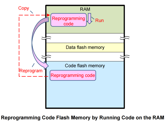
Copy the code to the RAM area for execution, including the code for erasing Flash and other code that needs to run normally while Flash is being erased and programmed, as shown in the figure below:
1.2
Specific Issues in OTA
In the OTA scenario, this single Bank architecture brings a series of challenges:
Issues
Impact
Requires downtime for upgrades
Business interruption (e.g., stopping motor operation), system unavailability, or performance limitations (most interrupts need to be intermittently disabled).
Risk of unexpected power loss during the upgrade process
If power is lost during the erase/write process, the MCU firmware may be corrupted, potentially bricking the device.
Lack of rollback mechanism
If the new firmware has bugs,
it cannot quickly revert to the old version,
and must be re-flashed.
Under this architecture, even if OTA is desired, a complex Bootloader process and verification mechanism must be designed, while carefully controlling power and upgrade timing, resulting in high overall development costs and low reliability.
2
Renesas’ Seamless OTA Solution
2.1
Why Dual-Bank?
If the MCU can have two independent program areas, one running the application and the other flashing the firmware, without interference, upgrades can naturally be achieved:
-
No interruption of existing business.
-
After writing the new firmware, switch the boot area with one click.
-
Even if the upgrade fails, it can automatically revert to the old firmware.
This is the revolutionary change brought by the Dual-Bank Flash architecture.
2.2
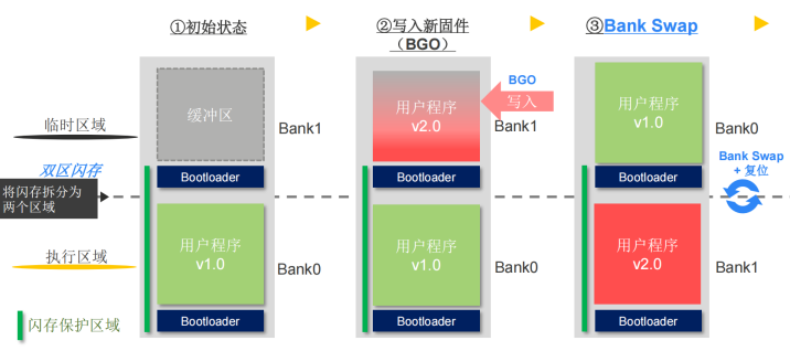
Overview of the Dual-Bank Solution
Renesas provides models supporting Dual-Bank architecture design in the RX series, RL78 series, RA series, etc., suitable for various application scenarios including industrial, automotive, and IoT.
In this article, we will detail the RX26T as an example:
-
The RX26T has 512 KB of Code Flash physically divided into Bank 0/1, each 256 KB.
-
Bank 0 runs the application normally, while Bank 1 erases/writes the new firmware in the background.
-
After the upgrade is complete, the boot settings are modified by switching banks, and a soft reset switches to the new firmware.
-
If the upgrade is interrupted or fails, it can flexibly switch back to the original Bank to ensure continuous operation of the device.
This mechanism allows the MCU upgrade process to truly achieve “seamless” operation, greatly enhancing system maintainability and user experience.
3
Setting Up the RX26T Seamless OTA Experimental Environment
3.1
Hardware Environment
-
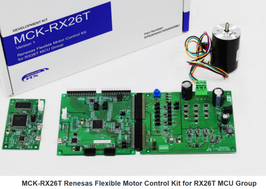
MCK-RX26T development kit
-
USB to UART tool for PC transmission of updated firmware
-
Logic analyzer to capture key test waveforms
3.2
Software Environment
-
IDE: e2 studio 2023-07 (23.7.0)
-
Compiler: CC-RX V3.06
-
BSP and related peripheral driver packages:
3.3
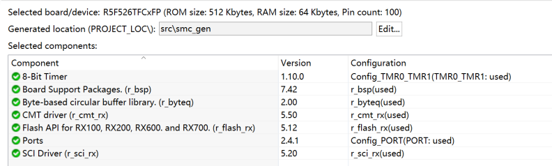
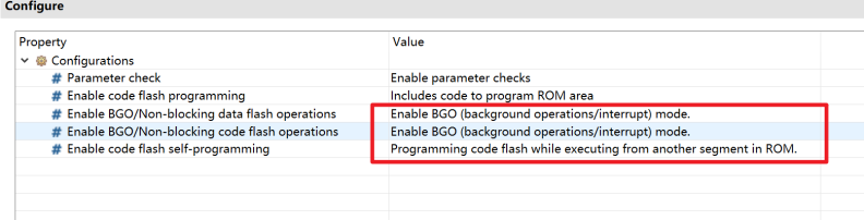
Flash Driver Configuration
To use the Dual-Bank function properly, the following configuration must be used in the Flash component, utilizing BGO mode, and allowing the self-programming library to run in Code Flash without needing to be copied to RAM.
3.4
Key Code Explanation for Flash Operations
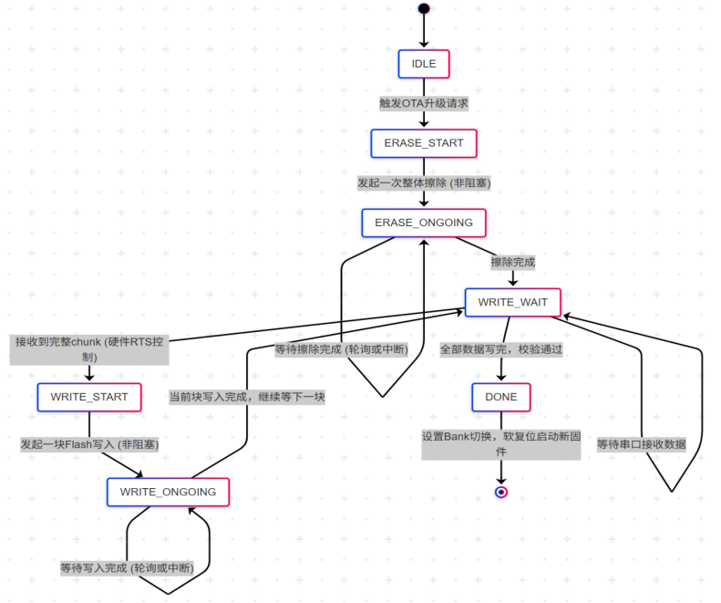
The Dual-Bank architecture can support the Flash operation library running in the background, allowing a callback function to be registered. When Flash completes erase and write commands, it directly enters background operation without blocking the main loop and interrupts.
-
During erase —> only initiate a complete erase once, and wait for the background flag to complete.
-
During write —> initiate a write for each block of data received, wait for the background flag to complete, and loop until all data is written.
Main code examples are as follows:
A
Flash Callback Function
Swipe left and right to view the complete content
void u_cb_function(void *event) { flash_int_cb_args_t *ready_event = event; switch (ready_event->event) { case FLASH_INT_EVENT_ERASE_COMPLETE: ERASE_COMPLETE_f = 1; case FLASH_INT_EVENT_WRITE_COMPLETE: WRITE_COMPLETE_f = 1; case FLASH_INT_EVENT_TOGGLE_BANK: break; default: break; }}B
Flash Initialization
Swipe left and right to view the complete content
e_fwup_err_t my_flash_open_function(void) { if (FLASH_SUCCESS != R_FLASH_Open()) { return (FWUP_ERR_FLASH); } #if (FLASH_BGO_MODE == 1) flash_interrupt_config_t cb_func_info; cb_func_info.pcallback = u_cb_function; cb_func_info.int_priority = 1; if (FLASH_SUCCESS != R_FLASH_Control(FLASH_CMD_SET_BGO_CALLBACK, (void *)&cb_func_info)) { return (FWUP_ERR_FLASH); } #endif /* (FLASH_BGO_MODE == 1) */ return (FWUP_SUCCESS); }C
Flash Erase Operation
Swipe left and right to view the complete content
static void fwup_erase_step(void) { if (!g_erase_started) { ERASE_COMPLETE_f = 0; R_FLASH_Erase(FLASH_CF_BLOCK_22, 22); g_erase_started = true; } else { if (!g_erase_done) { if (ERASE_COMPLETE_f == 1) { ERASE_COMPLETE_f = 0; g_erase_done = true; g_write_addr = BANK_LO_ADDR; g_write_offset = 0; g_total_writes_completed = 0; g_fwup_state = FWUP_STATE_WRITE; } } } }D
Flash Write Operation
Swipe left and right to view the complete content
static void fwup_write_step(void) { if (g_write_offset >= TOTAL_DATA_SIZE) { g_fwup_state = FWUP_STATE_DONE; return; } if (!g_write_in_progress && FWUP_UART_RTS) { uint8_t *buf = malloc(g_write_chunk_size); if (!buf) return; uint32_t chunk = (s_flash_buf.cnt >= g_write_chunk_size) ? g_write_chunk_size : s_flash_buf.cnt; memcpy(buf, s_flash_buf.buf, chunk); if (chunk < g_write_chunk_size) memset(&buf[chunk], 0xFF, g_write_chunk_size - chunk); WRITE_COMPLETE_f = 0; R_FLASH_Write((uint32_t)buf, g_write_addr, g_write_chunk_size); free(buf); g_write_in_progress = true; } else if (g_write_in_progress && WRITE_COMPLETE_f) { WRITE_COMPLETE_f = 0; g_write_in_progress = false; g_total_writes_completed++; g_write_addr += g_write_chunk_size; g_write_offset += g_write_chunk_size; if (s_flash_buf.cnt > g_write_chunk_size) { s_flash_buf.cnt -= g_write_chunk_size; memmove(s_flash_buf.buf, &s_flash_buf.buf[g_write_chunk_size], s_flash_buf.cnt); } else s_flash_buf.cnt = 0; FWUP_UART_RTS = false; } }3.5
Seamless OTA Process Diagram
4
RX26T Seamless OTA Experimental Test Results
4.1
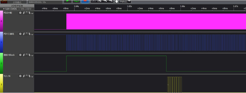
Logic Analyzer Test Waveforms
Added Test Code
-
In the main loop, toggle the IO port every 100us.
-
Toggle the IO port in the interrupt every 10us.
-
Toggle the IO port before and after entering the erase function.
-
Toggle the IO port before and after entering the write function.
The waveforms show that the overall operation has minimal impact on interrupts, with occasional short delays in the main loop during write operations, measured at around 25us, which is the preparation time before the Flash library enters BGO operation.
4.2
Motor Drive Performance Testing
To further validate actual performance, the motor drive was also included in the code, designing two software versions, where:
-
Version 1.1.1 starts the motor after power-up and controls the speed to 2000 RPM, printing information.
-
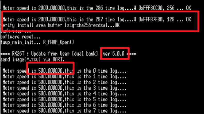
Version 6.0.0 starts the motor after power-up and controls the speed to 500 RPM, printing information.
First, burn version 1.1.1, and upon power-up, the motor runs normally, printing the following information:
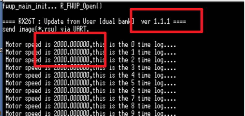
At this point, send the version 6.0.0 BIN file from the PC using Tera Term and enter the OTA process. It can be observed that the motor continues to run while continuously receiving the new firmware and writing it to the corresponding address in Bank 1. After the writing is complete, switch the bank and perform a reset. During the reset process, the motor will stop for a few seconds. Once the new software version starts, the motor will restart, accelerate, and control the speed at 500 RPM.
5
Experimental Summary
The Dual-Bank + BGO mode of the RX26T provides a perfect solution for firmware upgrades. The advantages of this approach are:
-
No impact on the current program during the upgrade process.
-
Prevents system “bricking” due to upgrade failures.
-
Safe and reliable upgrade process, supporting power loss protection.
-
Achieves a truly “seamless” upgrade experience.
This upgrade solution is particularly suitable for industrial control and motor drive applications that require high real-time performance, allowing firmware updates to be completed without affecting normal operations, making it an ideal choice for remote maintenance of industrial equipment.
6
Precautions
1
Key Points for Using BGO Mode:
-
Correctly configure the callback function during initialization.
-
Check the Flash status before each operation.
-
Use aligned buffers appropriately.
2
State Machine Design Principles:
-
State transition logic should be clear.
-
Individual state processing time should be short.
-
Use flags to track progress.
3
Debugging Suggestions:
-
Use GPIO to observe key timing.
-
Retain key log outputs.
4
Additional Notes:
-
The time to switch banks for software reset is very short, allowing the main function to run within 1 second.
-
If there are extreme requirements, such as core business processes needing to remain unaffected during OTA, there are solutions to copy core business processing functions and related interrupts to RAM before switching banks, thus avoiding the impact of software reset and achieving a seamless transition to the new firmware version.
Reference Documents and Examples
-
R01AN6850EJ0203-RX Family Firmware Update Module Using Firmware Integration Technology
-
r01an7203ej0100-rx-rx26t-ota-dualbank-firmware-update
-
R01AN3681EJ0120-RX Family Firmware Update Sample Program with Dual Bank Function, and Flash Module and SCI Module Firmware Integration Technology
-
R01AN2184EJ0522-RX Family Flash Module Using Firmware Integration Technology
-
R01AN6894EJ0100-RX Family Dual Mode Usage Guide
-
R01TU0346EJ0100–RL78/I1C (512KB) FOTA solution
What are the characteristics of multi-protocol industrial Ethernet IO-Link?
Analysis of Metering Applications for the RA4L1 Microcontroller

How to Develop MCU in VS Code