Follow+Star public account number, don’t miss the wonderful content
Author | Dmitry.GR
Translation | Zheng Liyuan, originally from | CSDN
For a long time, I have been trying to build a microcomputer that can run Linux with the least number of components. I have also attempted extreme simplifications and various interesting form designs, and this time I want to make a new attempt: to assemble a mini computer kit that can run Linux using only three 8-pin STM32 chips in the simplest way.1. Design a “minimized” minimalist computer
(1) Initial Concept
Once upon a time, people could buy DIY kits and assemble devices at home that could rival commercially available computers—but now, that era is long gone.
Today’s computers consist of hundreds or thousands of complex large chips, which not only lack publicly available data sheets but also require hundreds of watts of power through complex power transmission topologies. Moreover, modern operating systems have increasingly stringent hardware requirements: GB-level RAM, TB-level storage space, always-on network connectivity… it seems designed to “better monitor you”.
So the question arises: is it possible to assemble a modern computer at home? I believe that as long as it can run Debian Linux, use the vi editor, compile with gcc, and execute the make command, it is already “modern” enough—thus, this became my goal.
Based on my previous explorations, I know that this actually does not require very high specifications: 8MB of RAM + 1 MIPS (million instructions per second) processing capability is sufficient. Storage is even simpler; SD cards have long been able to easily meet capacity requirements. Although most modern computers no longer have serial ports, for embedded systems, serial ports are still the simplest interface, and USB to serial can replace traditional serial ports.
Therefore, my final goal is set as follows: at least 8MB of RAM, at least 1 MIPS processing capability, SD card storage, USB interface (for serial communication).
In terms of hardware design, I hope to design a computer that can be easily soldered and assembled at home, allowing even those with almost no soldering experience and just a RadioShack 45W soldering iron to do it. The whole machine should be compact, cute, and low-cost. To reduce soldering difficulty, I decided to use only 8-pin chips, which is also a fun challenge. Since each chip must retain at least power and ground pins, a maximum of 6 pins can be used for functionality. This limitation greatly impacts the entire circuit design and creates many constraints.
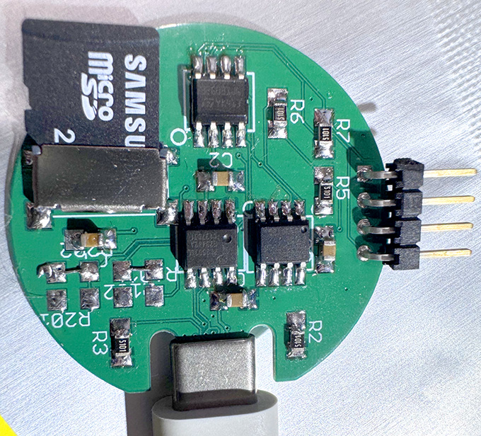
In terms of appearance, I decided to design it as a small round circuit board, with a USB-C interface set at the top edge, as shown in the figure below. This is the final version that works properly, and it was indeed soldered by me using a RadioShack 45W soldering iron!
(2) Component Selection
In fact, there are almost no 8-pin chips that support USB communication, but if I had to say, there should be “one and a half”.
The first is a truly usable solution: PL2303GL. This is a very compact and practical USB to serial bridge chip that requires no external components and can also output an additional 100mA of 3.3V regulated voltage, which is very convenient! Its performance fully meets expectations, and I personally like it very much. Prolific also provides driver support for almost all mainstream and niche operating systems. The only slightly troublesome part is that on macOS, these drivers need to be installed from the App Store, but the whole process is still relatively simple. It is worth mentioning that its predecessor model PL2303SA can actually be used, but since it has been discontinued (EOL), I do not recommend it.
So what does “half a chip” mean? This brings us to the V-USB project, which allows ATTINYx5 series chips to also achieve USB communication functionality. Although it only supports low-speed USB and consumes a lot of CPU resources, it can indeed work. The problem is that existing USB to serial protocols generally require BULK transfer endpoints, while the USB specification explicitly prohibits the use of BULK endpoints in low-speed devices. If we want to fully comply with USB standards, we would have to design a communication protocol using interrupt endpoints and write drivers for all mainstream operating systems—this workload is simply too large, and I am not interested. Fortunately, all mainstream operating systems do not strictly enforce this rule; even if low-speed USB devices use BULK endpoints, they can still be recognized and communicate normally. Therefore, we can directly use V-USB to simulate serial devices (ACM interface), which can basically work.
As for the choice of RAM, there is really no hesitation; SOIC-8 packaged PSRAM is the most suitable solution. Common suppliers include ISSI, APMEMORY, and Vilsion, who have been promising to release 16MB PSRAM chips for over a year, but have yet to fulfill that promise, so they are likely just making empty promises. Fortunately, 8MB chips are abundant and inexpensive, and can be purchased for just a few dollars on major e-commerce platforms. Therefore, I ultimately decided to use an 8MB RAM to build this Linux mini computer.
The last question is: which microcontroller to choose? Through parameter filtering, I finally focused on the STM32G0 series. In theory, STM chips should be the last choice because they never seriously release complete and accurate errata. The STM32G030 was the first to be eliminated because one of its pins is hardwired as RESET, leaving only 5 I/O, which is too limited. The STM32G031J4M6 looks okay; it is a relatively new chip, and maybe STM has filled in various pitfalls this time? Moreover, this project plan will not use too many on-chip peripherals, so it might be okay? 32KB flash, 8KB RAM—these two numbers crush all other options! The Cortex-M0+ core also makes it one of the strongest candidates in terms of performance. Official data shows that this chip has a frequency of 64MHz, and with a little effort, it can reach 80MHz, and with more effort, it can even run at 150MHz. Assuming I can avoid the various known/unknown bugs in the errata, this is undoubtedly the strongest choice—although I am not a fan of STM, I have no choice but to go with it.
2. Hardware Design
(1) Console
The UART pins are almost impossible to reuse with other functions. Attempting to reuse the RX pin of the UART poses a risk of data loss—when “other functions” are running, if serial data arrives at that moment, it will be missed. Reusing the TX pin of the UART is also unreliable: no matter how fast the “other functions” switch, as long as a low-level pulse is generated, the PC may misinterpret it as a serial character. If it is a brief low level, the PC usually recognizes it as 0xFF.
Theoretically, enabling parity could mask these interferences, but this is not a reliable solution. Moreover, who still uses parity in 2025? Ultimately, UART pins are not suitable for reuse with other functions due to the lack of higher-level protocols, chip select signals, or independent clocks.
So, 2 of these 6 pins are already occupied. I can only reluctantly accept this reality…
(2) RAM
All SPI PSRAM chips support QSPI mode to improve transmission speed. Unfortunately, QSPI requires 6 pins, and now only 4 are left. Fortunately, most PSRAM also supports dual-line SPI mode, where MOSI and MISO transmit simultaneously, sending 2 bits of data in one clock cycle, which is twice the rate of ordinary SPI. Even better, it does not require more pins than ordinary SPI and can share the SPI bus with other devices—because when not selected (deselected), these devices will not drive MISO or attempt to read MOSI.
However, the STM32G031 does not natively support dual-SPI. If you want to use it, you can only implement it through software simulation. But the question arises: can the software implementation of dual-SPI match the speed of the hardware SPI module? The hardware SPI module can run at half the CPU clock rate and connect to the DMA unit for continuous data transfer.
To achieve the same throughput with pure CPU simulation, each transmission cycle must consume only 4 instruction cycles, which is almost the CPU’s limit; any faster is impossible. Since the fastest is only “barely catching up” with hardware SPI, why bother? Conclusion: RAM should still be accessed using ordinary SPI. However, this directly uses up the last 4 pins.Alas…
(3) SD Card
So the situation has become tricky: no pins are left, but I still need to connect an SD card.
SD cards can use SPI communication, requiring only one more pin for the chip select signal, but there are no extra pins left. I considered several solutions, the simplest being to connect an inverter to the nCS of the RAM and use its output as the nCS signal for the SD card. I prototyped this idea and found that it worked quite well. However, there are two issues: first, some SD cards cannot accept the situation of “selected but no data sent”. If there is no data written between two RAM accesses, it appears to the SD card as an abnormal operation, posing compatibility risks. The second is that the inverter requires an additional IC or at least a transistor, which increases BOM complexity. For beginners who want to DIY this board, the more components on the board, the more difficult the assembly becomes. Therefore, this solution was labeled as the “worst-case scenario” and temporarily set aside; I still need to look for better solutions.
Since the data output rate of this device is not high, the UART baud rate can actually be set quite low. So I considered: can the TX pin of the UART be added with a low-pass filter and then used as the nCS for the SD card? As long as the SD command is short enough and the clock frequency is high enough, the selection signal’s time window can be “passed” by the filter. This method is theoretically feasible but practically very fragile. I further calculated that to meet the SD protocol initialization requirements, the UART baud rate must be as low as 300bps or lower, and even so, if the SD card’s response speed is slightly slow, the system is likely to crash because the SD protocol explicitly prohibits canceling the chip select signal during the response reading process.So this solution is even worse than the first.
Just as I was about to return to the initial “worst-case scenario,” a crazier idea suddenly popped up: does RAM mind being selected and then immediately deselected without executing any commands or data transfers? Experiments showed: it does not mind; this test passed on all SPI RAM chips!
Why? Because SD cards support not only SPI but also the SDIO protocol. SDIO does not use 4 unidirectional lines but instead uses 1 clock line (CLK) and 2 bidirectional lines (CMD and DAT). If in 4-bit mode, it would add 3 DAT lines, but in this project, only 1-bit mode is needed. Although the SDIO protocol is not detailed in the public SD specification, it can be inferred through observation—this solution, while not saving many pins, brings new possibilities for combinations.
So the question becomes: can the 3 signal lines of SDIO be reused with the RAM pins? After repeated deductions, I finally found a “feasible mapping”: RAM’s nCS → SD’s CLK; RAM’s CLK → SD’s CMD; RAM’s MOSI → SD’s DAT. Analyzing their access behaviors, I found that when accessing RAM, the SD card sees CLK pulled low, and when RAM is deselected, CLK is pulled high. The RAM’s SPI is set to Mode 3, where CLK is idle high, so each access to RAM appears to the SD as if a “1” bit was sent on the CMD line. This corresponds perfectly to the idle state of the command gap in the SDIO protocol, making it safe.
Similarly, the SD card does not read or write the DAT line between commands, so the RAM’s MOSI signal will not be misinterpreted. Conversely, when accessing the SD card, CLK and CMD, DAT need to be switched, which is just a quick selection and deselection for RAM—RAM can also accept this behavior. Perfect!
It should be noted that the premise of this solution is that SD card transactions must be “completed in one go”; RAM cannot be accessed during this process. This means that multi-block read/write cannot be used; considering the current pin-tight situation, this is acceptable.
Alright, this is a potentially feasible solution! Next is experimental verification, and the result is—success!Of course, since the STM32G031 does not have the corresponding hardware module, the SDIO access is completely implemented via bit-banging.Ultimately, the assembly code I wrote achieved a transmission efficiency of 14 CPU cycles per bit, and overall performance is still quite good.
(4) Back to the Console
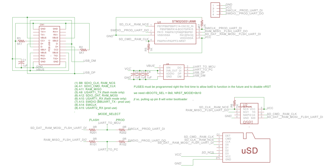
Now all I/O interfaces can theoretically fit into 6 pins, and it’s time to officially assign functions to each pin.
Some pin functions have already been determined: RAM will use standard SPI, and the corresponding lines will be reserved for it. The SD card shares these lines and does not require additional allocation. The remaining pins 7 and 8 are exactly the SWD debug interface, which is very convenient for debugging in the early stages of development. Additionally, through the process of elimination, they also need to serve as the serial port. Pin 8 can serve as USART2.TX, and by enabling the USART’s “pin swap” feature, it can be converted to USART2.RX. Because UART reception is troublesome without hardware assistance, pin 7 is reserved for TX. This pin does not support any alternative functions of USART, but that’s okay; we can implement UART sending manually using bit-banging.
Interestingly, when considering the shared pin scheme earlier, I was thinking of making the UART as slow as possible; now, to manually implement UART, the baud rate needs to be as fast as possible—because during sending, the CPU must focus on “watching the send” and cannot be interrupted. Sending each character (at 115200bps) takes about 87 microseconds. Theoretically, we could also send each character bit by bit through timer interrupts, but the timing jitter caused by interrupts could lead to serial errors. Fortunately, in most cases, devices do not output frequently, so this solution is already quite good. The UART sending bit-bang implementation works well, the pin allocation is complete, and we can now enter the software development phase.
But you might ask, what about the initial programming? Under this “unconventional pin layout”, how could the official STM32 bootloader possibly support it? It indeed does not support it, so I designed 4 solder bridges on the board, allowing the connection method of the serial port to be switched through jumpers: in “development mode”, the bootloader is available, but RAM and SD cards cannot work; in “production mode”, the ROM bootloader is disabled, but the project can start normally. Fortunately, this project comes with a custom bootloader, so after the initial programming, there is no need to rely on the ROM bootloader anymore.
3. The Story About Software
(1) Emulator
Before the project started, I had already written a MIPS emulator that can boot Linux, and the entire code is written in ARMv6M assembly language, so reusing this part of the code in the new project is not difficult.
To further improve performance, I also wrote a JIT (Just-In-Time) compiler from MIPS to ARMv6M, which performed well. Unfortunately, this JIT compiler is too large, with the compiled code being 46KB, while the translation cache available in this project is only 6KB, so the performance improvement is not significant. Ultimately, I chose to temporarily set aside this JIT for future use.
In this project, the 32KB flash of the STM32G031 chip is divided into two areas: 8KB allocated for the bootloader and 24KB for the main application. Aside from some necessary optimizations and adaptations, the main emulator code remains largely unchanged.
(2) Bootloader
So why is a bootloader needed? The reason is quite simple: there are no extra pins on the board for debugging; the project is still in the development stage and needs a way to upgrade firmware, fix bugs, or add new features. The most direct and effective solution is to design a bootloader that supports SD cards, can recognize the FAT file system, and automatically upgrade the firmware when a new version is detected.
The reason the bootloader size reaches 8KB (actually 6.5KB, but rounded up to 8KB due to the flash block size of 2KB) is that it must include a complete SDIO driver, FAT file system driver, flash writing code, and a lot of logging to troubleshoot various issues during updates. Of course, it also embeds a UART sending module implemented via bit-banging. The bootloader checks the value at offset address 16 in the main program image, which is the version number of the main program. Only when the version number in the update file is higher than the current main program and passes some basic checks will the update be executed. As for the version number of the bootloader itself, it is recorded at offset address 8, only for displaying startup information. The firmware update file that meets the conditions is named FIRMWARE.BIN, and once verified, it will be applied.
The bootloader runs after the chip is reset, with a default frequency of 16MHz. The frequency during the main program’s operation is adjustable, allowing users to attempt overclocking. However, frequently modifying code, recompiling, and programming firmware is too cumbersome. This issue can be easily solved with a small trick: since the bootloader has already mounted the FAT file system for checking updates, it can also scan for files or folders named CLOCK. If present, the number following it will be parsed as the running frequency of the main program (in MHz). If this value is out of the reasonable range (32–200MHz) or the related file cannot be found, it defaults to 132MHz.
(3) SD Card Partition and Boot Process
Like my previous projects based on the MIPS emulator, the boot process of this project also borrows from the design of the PC boot process. The system first reads the first sector of the SD card, loads it into the first few bytes of memory, and then jumps to execute; this first-stage boot code will continue to look for a partition of type 0xBB and load it completely into memory address 0x80001000, then jump again; at this point, the second-stage bootloader starts running, which has logging and serial output capabilities; it will scan all partitions, find the one marked as “active”, and attempt to mount it as a FAT16 file system; if a file named VMLINUX exists in that partition, it will load it as an ELF file and jump to its entry address; if that file is a valid Linux kernel, it will enter the Linux system boot process.
The startup parameters (command line) passed to the kernel are hardcoded in the bootloader and do not support dynamic modification. It specifies that the kernel will use /dev/pvd3 as the root file system and /sbin/uMIPSinit as the init program, while also attempting to mount /dev/pvd1 as the /boot directory.
Careful reading of the above shows that although the system requires the root file system to be in the third partition (pvd3), there is actually no strict requirement on the order of other partitions—this is intentional design. For this project, the FAT partition is first, the bootloader partition is second, and the Linux root file system is third. Why? Because when inserting an SD card with multiple partitions, Windows and macOS will mount the first partition, while Linux will mount all partitions, which means:
-
The FAT partition can be easily accessed from the PC and can also be mounted to /boot by the Linux system after booting for file transfer and updates;
-
Both from the PC and from within Linux, the CPU frequency can be adjusted by modifying the CLOCK file, greatly enhancing flexibility.
Before the bootloader begins any operations, it will first quietly wait for 6 seconds. This delay occurs before reconfiguring the pins, allowing users some time to connect a debugger (SWD), as the development board has reserved a 4-pin debug interface. After 6 seconds, the bootloader will reconfigure the pins, at which point the SWD function will no longer be available, and the debugger can no longer connect. Additionally, as a backup mechanism, the bootloader will also implement the following behavior by setting option bytes: if the BOOT0 pin (pin 8) is pulled high, the chip will boot from ROM; disable the chip’s RESET pin (used as a regular GPIO in this project) and BOR (Brown-out Reset, not used in this project). Once everything is ready, the bootloader will attempt to initialize communication with the SD card, check for update files, and finally officially start the system.
4. How is the performance?
The official maximum operating frequency of the STM32G031 is 64MHz, so why are we discussing running it at 150MHz here? The reason is: as long as some “black technology” is appropriately applied, the STM32G031 actually has very strong overclocking capabilities. The CPU core voltage of the STM32G031 is powered by an internal regulator, and this voltage can be adjusted through the PWR->CR1 register. ST’s official documentation mentions two voltage settings: VOS2 (corresponding to 1.0V Vcore), under this setting, the chip can only run at 16MHz; VOS1 (corresponding to 1.2V Vcore), under this condition, the chip can only run at 64MHz.
Actual tests show that in VOS1 mode, the STM32G031 can stably run at around 75MHz, which is already a good overclocking result, but not stunning. However, early documentation (and information on similar series chips) also mentioned VOS0 mode, corresponding to 1.35V Vcore. What happens if we forcibly try to enable this voltage mode? The result is surprising— it really works, and the overclocking potential is greatly increased: most chips can still run stably at 136MHz, and some exceptionally good chips can even reach 180MHz! Of course, the access speed of Flash does not increase synchronously with the frequency, so the wait state for Flash must be set correctly, although this will affect some speed improvements, but overall it is still worth it.
At a frequency of 148MHz, this STM32 simulates running a MIPS CPU, roughly equivalent to a 1.65MHz MIPS R3000 (FPU disabled). It is not a performance monster, but it can boot in about a minute, and tools like vi, make, objdump, and gcc can work normally—this is a complete Debian system, and you can even import .deb packages through the /boot directory and install them, everything can run smoothly.
5. Final Assembly!
(1) Obtaining Parts
You can choose to buy the parts yourself and send the PCB to your favorite factory for soldering. Additionally, we are also looking for partners to package and sell kits; if you have relevant leads, please contact me—this could be a great DIY gift!
(2) Initial Soldering
Next is the part you are most concerned about: how to solder this board yourself. The board you have has been designed to be as easy to assemble as possible. We recommend the following soldering order:
-
First, solder the SD card socket, aligning the position, solder one pin at a time, and then solder the four fixed corner pins (be patient while soldering);
-
Solder all capacitors, a total of 4, and they all have the same value, making them easy to identify, and install them in positions C1~C4;
-
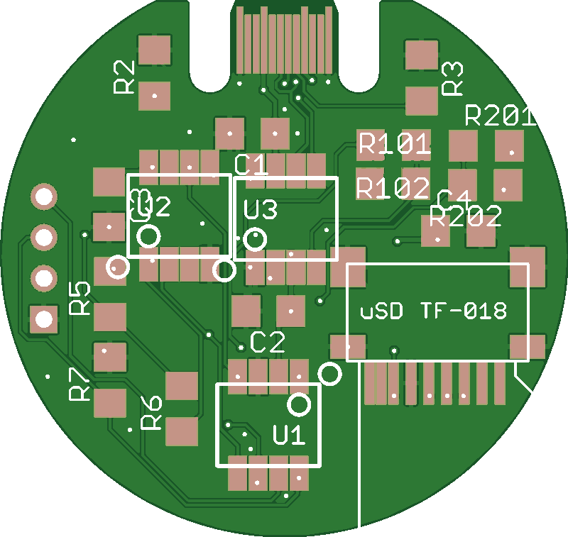
Solder all resistors, which also have the same resistance value, and install them in positions R2 ~ R7 (note: there is no R4); do not solder R101, R102, R201, R202 for now, as these will have other uses later;
-
Solder the main control chip STM32G031J6, placing it in the position marked U1, and the orientation is very important (the first pin has a small ST logo mark, corresponding to the small dot on the PCB);
-
Solder the USB to serial chip (PL2303GL), placing it in the position marked U3. On this chip, pin 1 is usually marked by a small pit on the top of the chip, align it with the mark on the board and solder it.
(3) Secondary Soldering
This stage is to program the STM32 with the bootloader. For this, you can download the programming tool provided by STM (Windows users can use the official flasher, while other systems can use the open-source stm32flash tool). Prepare a USB-C cable, and use two thin wires to bridge the positions marked R101 and R201 on the circuit board, ensuring that the SD card is not inserted and the RAM chip has not yet been soldered. Then, connect the board to the computer via USB-C, and the system should recognize a virtual serial port, using the programming tool to write the BOOTLOADER.BIN file (the path and serial port name depend on the system).
After programming is complete, remove the soldering wire used to bridge R101 and R201, and connect R102 and R202 instead, which is also the final correct configuration for the serial port pins. Finally, solder the RAM chip (APS6408 or VTI7064, position U2), and the pin 1 of this chip also has a small pit mark, align it with the small dot on the PCB and solder it. Thus, the hardware assembly is complete!
6. Program the Main Firmware and Complete the First Boot
We need to use a disk image writing tool to write the provided system image to an SD card with a capacity of at least 1GB, as follows:
(1) Windows: Use [Win32 Disk Imager];
(2) macOS: Use the built-in “Disk Utility”;
(3) Linux: Use the dd command.
This system image already contains the complete boot process: including the first-stage MIPS bootloader, the second-stage MIPS bootloader, the partition containing the Linux kernel and firmware, and a Debian root file system (rootfs).
After the image writing is complete, eject and reinsert the SD card, and the computer will recognize and mount the FAT file system partition. At this point, please copy the main firmware FIRMWARE.BIN from the downloaded package into the FAT partition of the SD card. This step allows the bootloader to automatically recognize and program this firmware during the first boot. If you have not recompiled the firmware, this step can actually be skipped, as the image itself already contains this file. However, even repeating this operation will not have any side effects, so feel free to execute it—thus, everything is ready!
Insert the SD card, reconnect the USB-C data cable to the computer, open your favorite serial terminal software, and configure it to 115,200 bps, 8N1 format. After a few seconds, you will see the serial terminal start printing boot information, which is the process of multiple boot stages executing sequentially. During the first boot, the STM32’s fuses will be written with configurations, and you may need to unplug and reinsert the USB-C connector once when the serial information stops. Since the fuses are non-volatile, this only needs to be done once. After about 20 seconds, you will see the Linux kernel booting print information; the entire boot process takes about 1 minute, and eventually, you will see a shell prompt. Considering that the system only has 8MB of memory, it is recommended that you first execute the swapon /swapfile command to enable swap space, which takes about several tens of seconds to complete, after which you can run more commands and programs!
Finally, interested developers can download this compressed package: https://dmitry.gr/images/uMIPS.8PL.zip, which contains all the content needed for this project, looking forward to your DIY journey!
Original link:
https://dmitry.gr/?r=05.Projects&proj=36.%208pinLinux
———— END ————
● Column “Embedded Tools”
● Column “Embedded Development”
● Column “Keil Tutorials”
● Selected Tutorials in Embedded Column
Follow the public account reply “Join Group” to join the technical exchange group according to the rules, reply “1024” to see more content.
Click “Read the original” to see more shares.