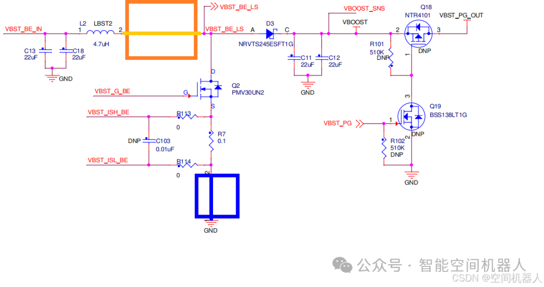
 This circuit diagram describes a boost converter circuit used in back-end power systems, aimed at raising the input low voltage to the required output voltage. Below is a detailed explanation of each part and its function:
1. VBST_BE_IN (Input Voltage)
- Function
: This is the input voltage of the boost converter. It typically comes from a low voltage source, such as a battery or other low voltage power supply. The input voltage will be boosted to the desired output voltage through the boost converter. - Detailed Description
: The stability of the input voltage directly affects the efficiency and output stability of the boost converter. The input voltage may fluctuate, and the boost converter needs to adjust its operating state based on this input voltage. Many PMICs on various platforms can both step-up and step-down voltage; when the input voltage drops to a specified range, it boosts, and when it exceeds the target voltage, it steps down, automatically adjusting through peripheral circuits and control.
2. L2 (4.7μH) (Inductor)
- Function
: L2 is an inductor in the boost converter, primarily used for energy storage. It generates a magnetic field through changes in current, and when the switch operates, the inductor converts the magnetic field into electrical energy and transmits it through other components. - Detailed Description
: The inductor is one of the critical components in the boost converter. Its role is to store energy during the switch cycle and release that energy when the switch is off, thereby increasing the output voltage. The selection of the inductance value significantly impacts the efficiency, size, and response speed of the boost converter, along with parameters such as saturation current and temperature rise current.
3. C13, C18 (22μF) (Input Filter Capacitors)
- Function
: These two capacitors are filter capacitors at the input, used to smooth the input voltage and reduce voltage spikes and noise. - Detailed Description
: The input voltage of the boost converter may have noise or rapid fluctuations, especially under other loads. Capacitors C13 and C18 filter these fluctuations, ensuring that the inductor and switch circuit can receive stable voltage input, thus improving the overall stability and efficiency of the circuit, mainly focusing on ESR, temperature curves, etc.
4. D3 (NRVTS245ESFT1G) (Schottky Diode)
- Function
: D3 is a Schottky diode, primarily providing a unidirectional conduction path for current. It helps direct the energy from the inductor to the output. - Detailed Description
: The Schottky diode has a low forward voltage drop and fast switching characteristics, making it ideal for boost converters as it reduces losses and increases efficiency. It conducts when the inductor releases energy, ensuring that energy can smoothly flow to the output, with selection mainly considering current headroom and specific verification based on load and temperature conditions.
5. Q2 (PMV30UN2) (MOSFET)
- Function
: Q2 is a field-effect transistor (MOSFET) that controls the flow of current. In the boost converter, the MOSFET primarily controls the current flowing through the inductor during the switch cycle. - Detailed Description
: Q2 controls the energy storage and release process of the inductor L2. Its switching state determines when the inductor stores energy (switch on) and when it releases energy (switch off). During this process, the performance of the MOSFET directly affects the efficiency and response speed of the circuit.
6. R7 (0.1Ω) (Sensing Resistor)
- Function
: R7 is a small 0.1Ω resistor, typically used for current sensing or detection. It monitors the current flowing through the inductor or other parts of the circuit. - Detailed Description
: By adding a small resistor in the current path, the current value can be inferred from the voltage drop that occurs when the current flows through it. This current information can be used for control feedback systems to ensure the boost converter operates within safe limits. For example, if the current is too high, it may trigger a current limiting mechanism to protect the circuit from damage, with selection mainly focusing on power, precision, etc.
7. C11, C12 (22μF) (Output Filter Capacitors)
- Function
: C11 and C12 are output filter capacitors, primarily used to smooth the output voltage after boosting. - Detailed Description
: The output voltage of the boost converter typically contains high-frequency noise or pulse ripple, which may affect downstream circuits. By adding these two large-capacity capacitors (C11 and C12), these high-frequency noises can be effectively removed, providing a more stable and cleaner output voltage. In DCDC boost circuits, such large capacitance (22μF) is very important as it helps maintain output voltage stability.
8. Q18 (NTR4101) and Q19 (BSS138LT1G) (MOSFETs)
- Function
: These two MOSFETs are used to control the output or feedback regulation part, helping to maintain the stability of the output voltage. - Detailed Description
: Q18 and Q19 act as switches in this circuit, adjusting the operating state of the boost converter to ensure the output voltage does not exceed the set range. They participate in feedback control at the output, or are used for over-voltage protection, over-current protection, etc., ensuring the boost converter operates stably under various working conditions, applied according to project needs, with the MOS front-end already having feedforward voltage sensed by the chip for control.
9. VBST_PG (Power Good Signal)
- Function
: VBST_PG is the “Power Good” signal that indicates whether the output of the boost converter is operating stably. - Detailed Description
: When the boost converter is operating normally, the VBST_PG signal is pulled high, indicating that the output voltage is stable and meets requirements. If an anomaly occurs, such as the output voltage falling below the set value, the VBST_PG signal will be pulled low, indicating a fault or abnormal state in the system. This is an important monitoring signal that helps the system assess the health status of the boost converter.