Hello everyone, I am EE Xiaoxin.
EEWorld user littleshrimp received an engine ECU from a scrap Volkswagen car. After his thorough disassembly, he discovered many common classic chips, as well as many unique design aspects.
(The original post comes from the EEWorld forum, welcome to enter the link to communicate with the author of this article: https://www.eeworld.com.cn/aaXLy9K)
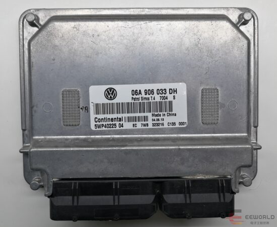
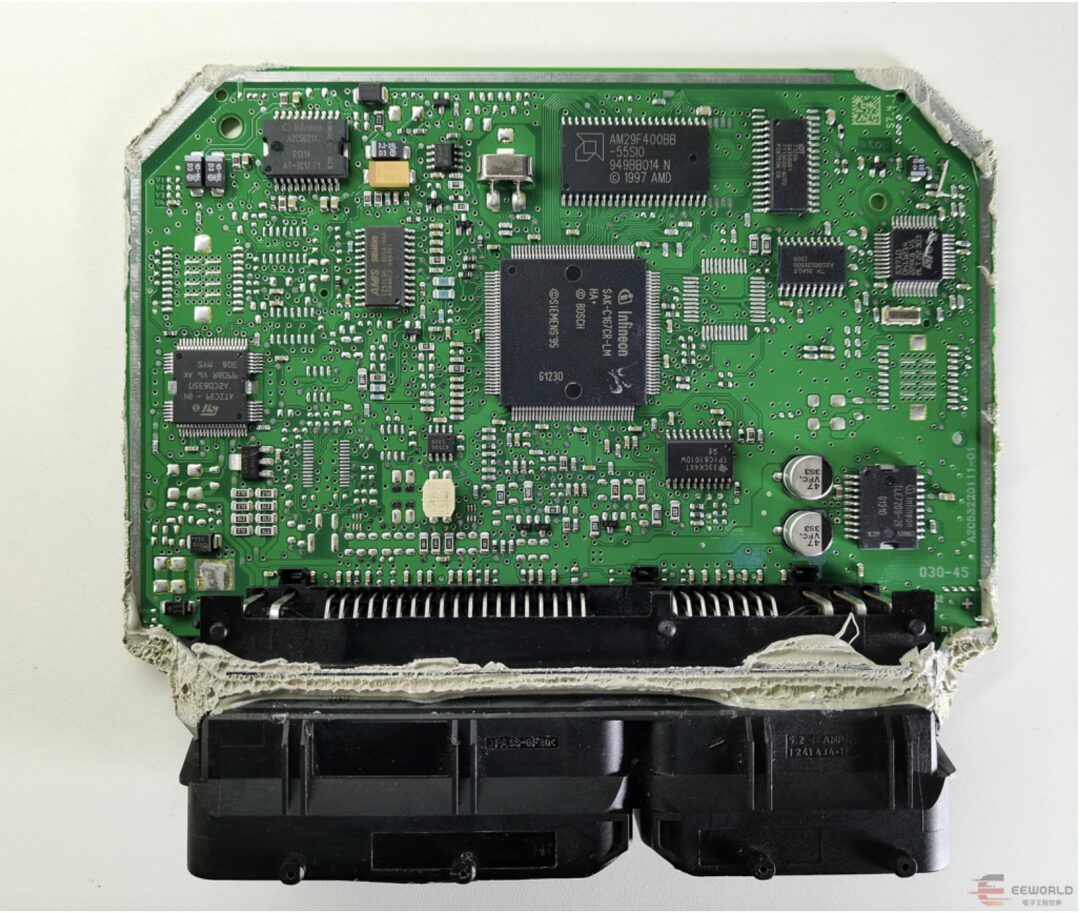
Disassembling the Volkswagen Engine ECU:
The lack of chips on the back is intriguing, while the combination of chips on the front showcases its complex functionality. The internal PCB layout presents a unique design; however, it is perplexing that some chips, especially most of the ST chips, lack data sheets, which greatly hinders a deeper understanding of their parameters and functions. Additionally, the method of fixing the crystal oscillator is different, using a base mount instead of the common soldering directly to the development board. Moreover, the device has numerous interfaces, but due to the unclear purpose of these pins, effective pin testing cannot be conducted, posing obstacles to further exploration of its working principles and application scenarios. Let's follow our disassembly to explore further!
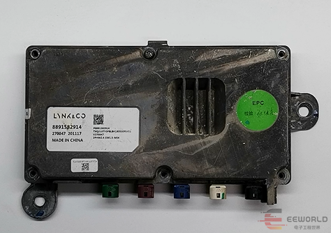
It is uncertain which model of car this device is applied to.
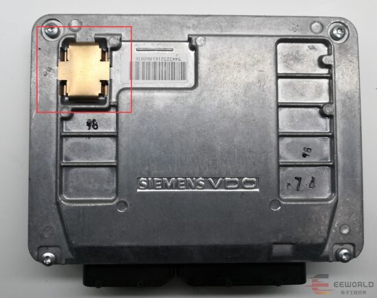
There is also a suspicious vent-like feature on the back.
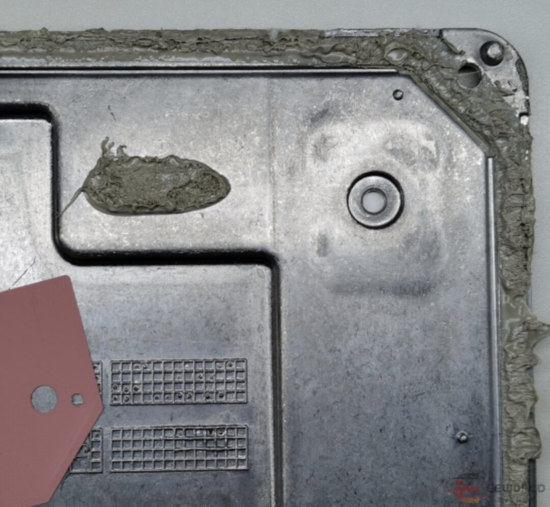
The shell of this device features a unique craftsmanship, surrounded by a large amount of gray sealing glue, which has retained good softness over the years. This may be to ensure that the internal components are protected from external environmental interference, providing waterproof, dustproof, and structural stability.
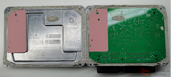
The back of the PCB has no chips; most of the chips below are from Infineon and ST.
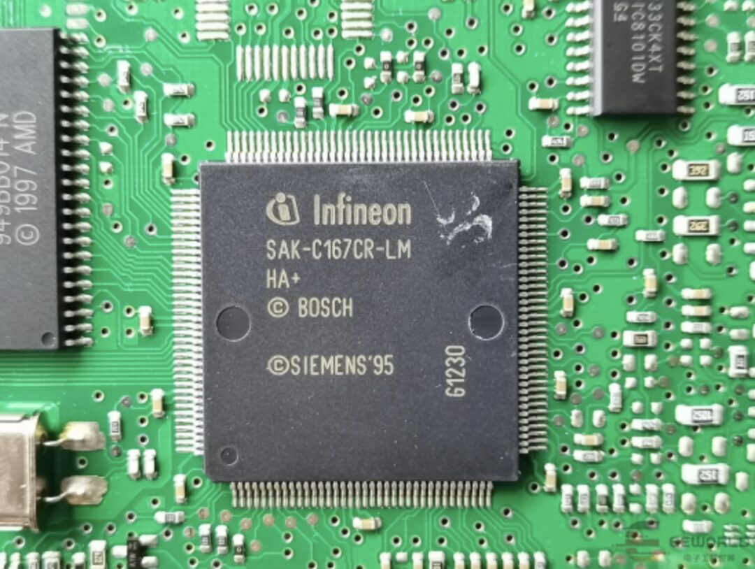
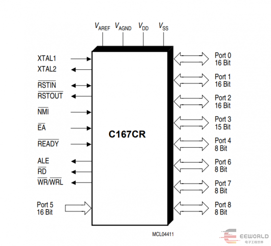
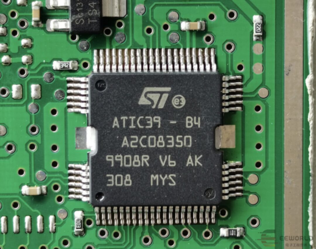
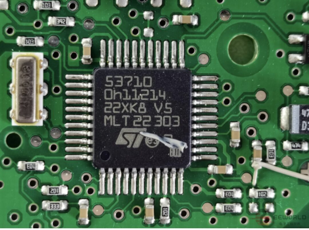
The main control chip uses Infineon’s C167CR scheme, which should be the core brain of the entire system, responsible for coordinating and controlling the operation of various functions.
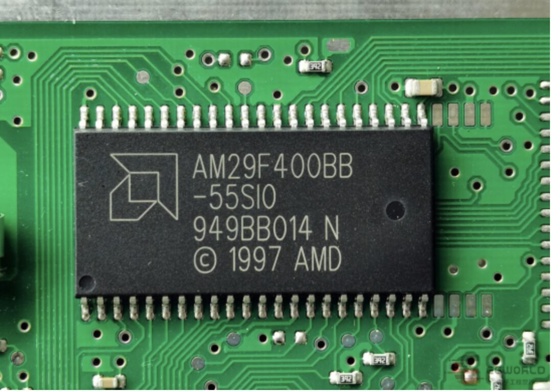
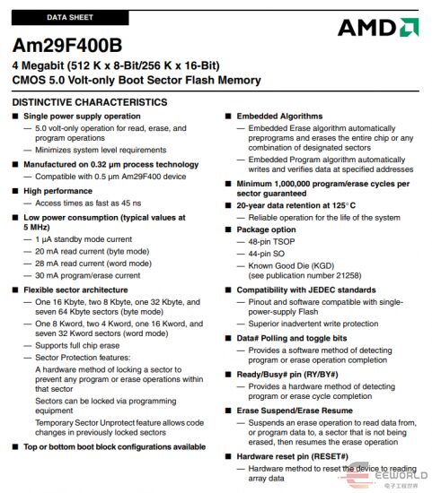
It is also equipped with an AMD 4Mbit FLASH.
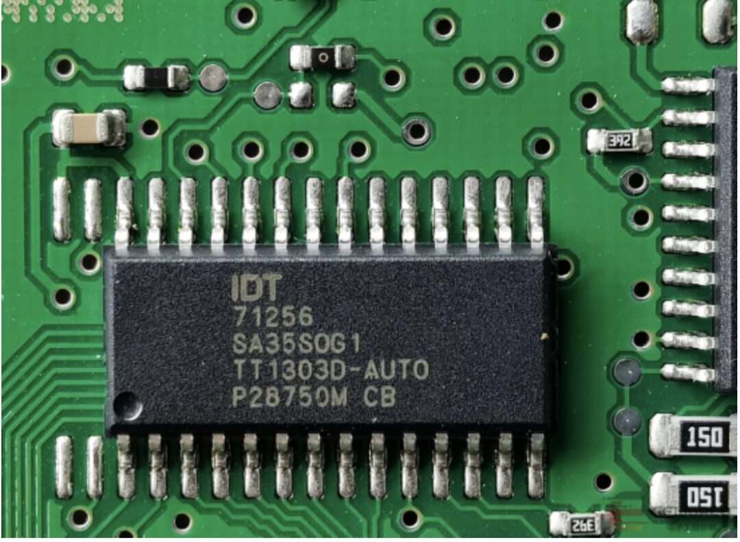
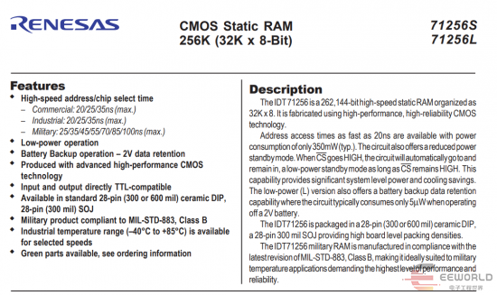
Used for storing programs and data; IDT (now acquired by Renesas) 256Kbit SRAM supports rapid read/write of data.
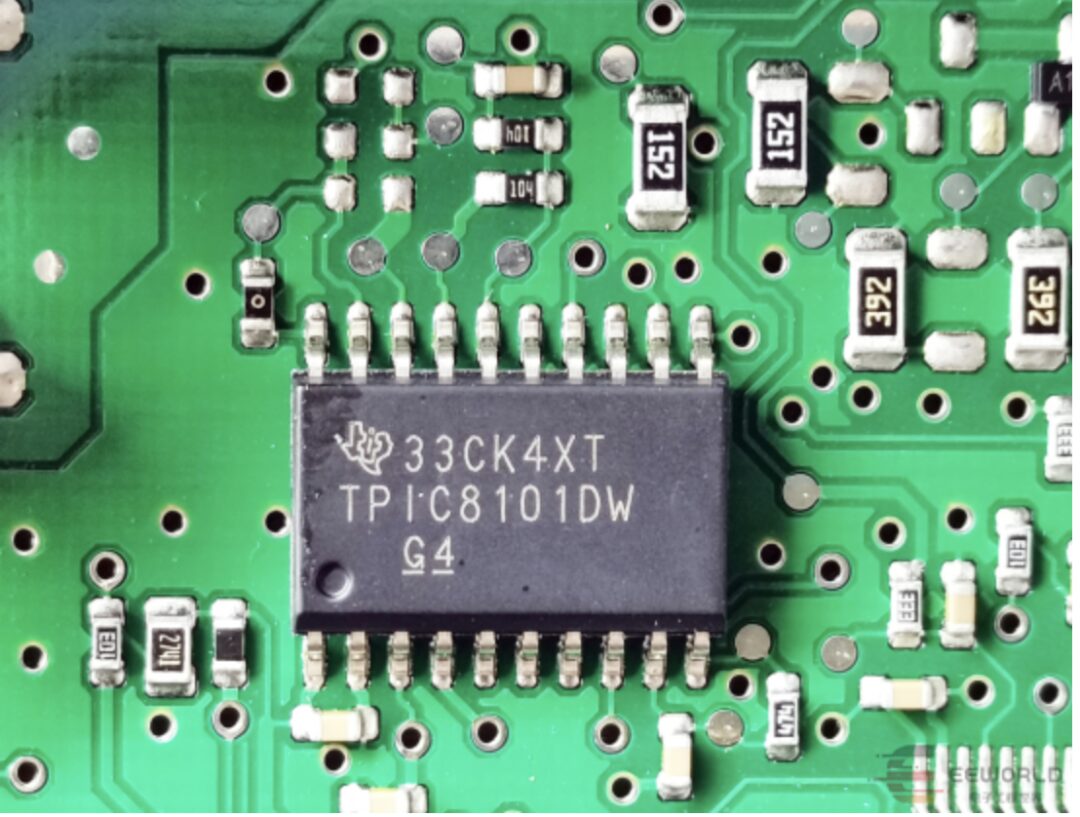
TI’s TPIC8101 serves as the interface chip for vibration and engine knock sensors, playing a key role in sensing the engine’s operational status.
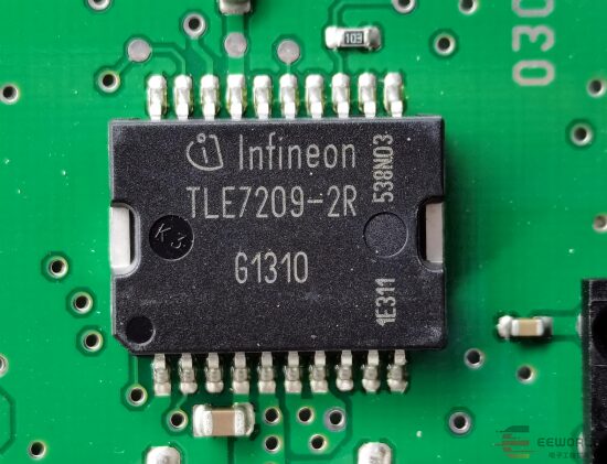
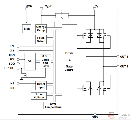
Various chips from Infineon showcase their capabilities, such as the TLE 7209–2R 7A H-bridge driver chip used to drive related components.
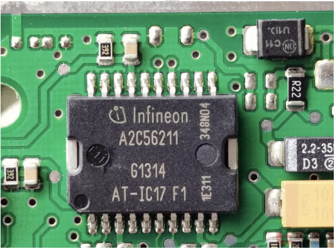
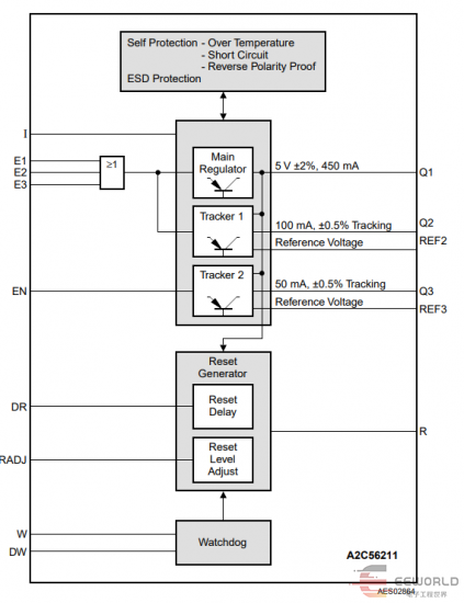
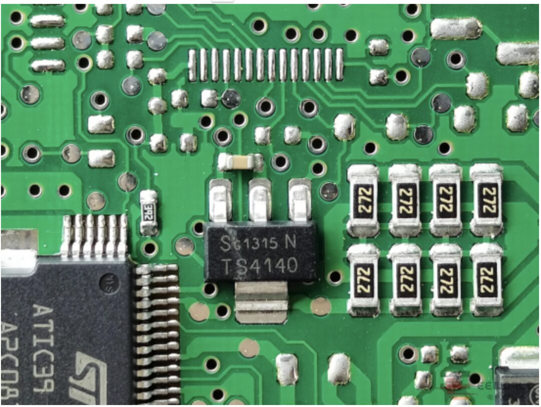
Infineon’s A2C56211 ultra-low dropout triple regulator ensures stable voltage supply.
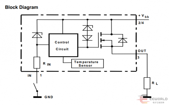
Infineon’s BTS4140N high-side power switch effectively manages power.
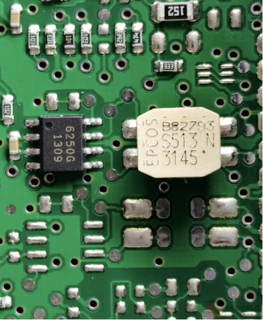
EPCOS’s telecom data line choke plays a filtering and anti-interference role, while Infineon’s TLE6250 high-speed CAN transceiver is responsible for data transmission.
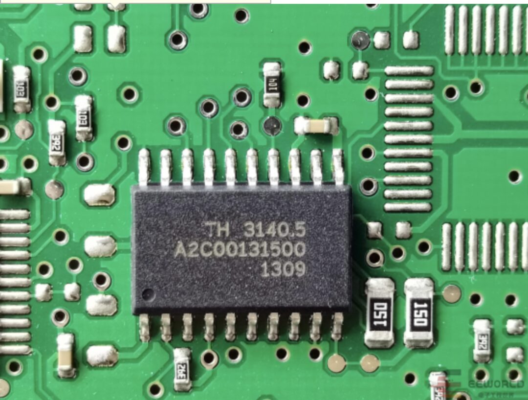
The rest are chips for which data sheets cannot be found.
It is strange that most ST chips also lack data sheets.
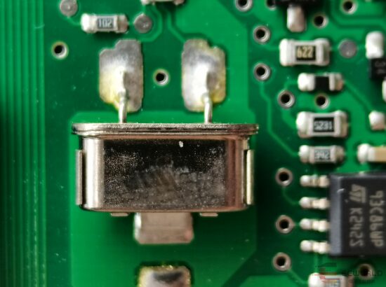
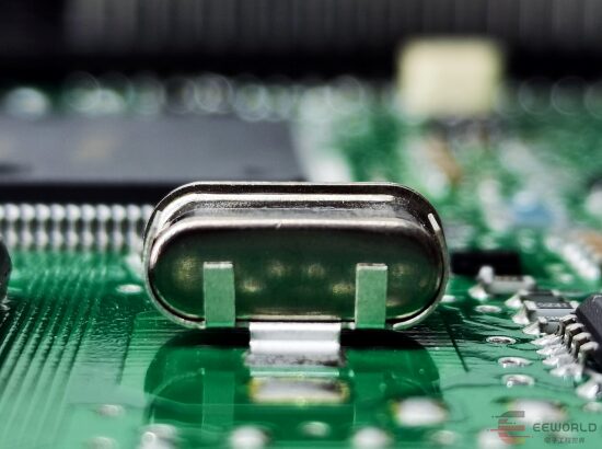
This crystal oscillator uses a base mount; previously, I saw development boards using a lump of solder directly.
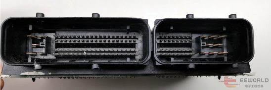
The interfaces are densely packed, and it is unclear what these pins are for, making testing impossible.
Although it is currently uncertain which model of Volkswagen this device is specifically applied to, this disassembly undoubtedly opens a window for us to understand its internal structure, laying the foundation for further research and analysis, and also igniting our enthusiasm for exploring its unknown functions and application areas, providing valuable references for the development of automotive electronic technology.
Disassembly Reveals Lynk & Co 360-Degree Imaging:
For drivers, blind spots during driving are undoubtedly a safety hazard that cannot be ignored. Fortunately, the 360-degree imaging system provides us with an effective solution. Its working principle is quite straightforward: the system captures images of the surrounding environment using multiple high-definition cameras installed around the vehicle, and then uses the onboard processor to synthesize these scattered images into a seamless panoramic view. This panoramic view is clearly displayed on the vehicle’s central control display or streaming rearview mirror. Additionally, the system offers a range of auxiliary functions, such as dynamic trajectory lines and distance prompts, to help drivers better grasp the situation around the vehicle.
 As a vehicle safety configuration, the choice of chips and technical solutions inside the 360-degree imaging system undoubtedly arouses our strong interest. Today, we will disassemble a Lynk & Co brand 360-degree imaging computer to satisfy everyone’s curiosity about the secrets behind this technology.
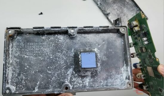
This is a Lynk & Co 360 imaging computer that has been exposed to water, with most screws already removed by someone else.
After opening the shell, the internal rust is quite severe.
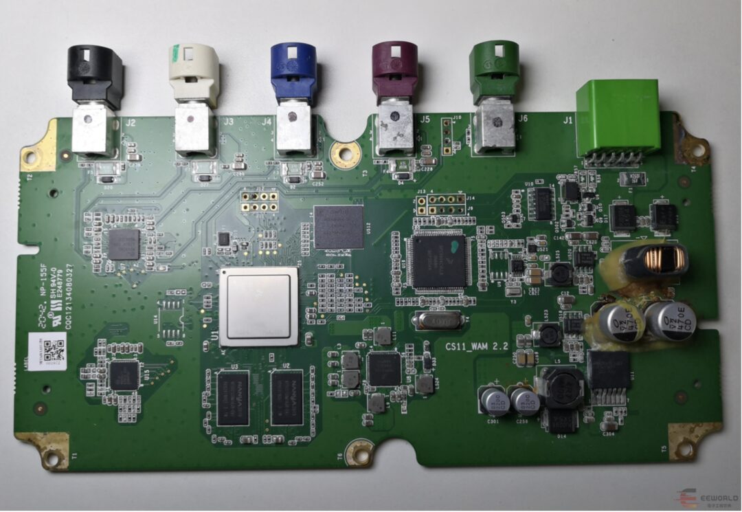
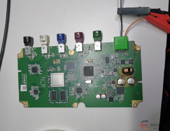
The board supports four camera inputs and one display output interface, using the NXP solution overall. After being washed with tap water, it looks quite nice.
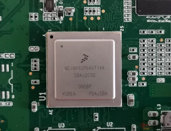
The video processor is MCIMX6DP6AVT1AA, an NXP i.MX 6DualPlus Automotive Applications Processor.
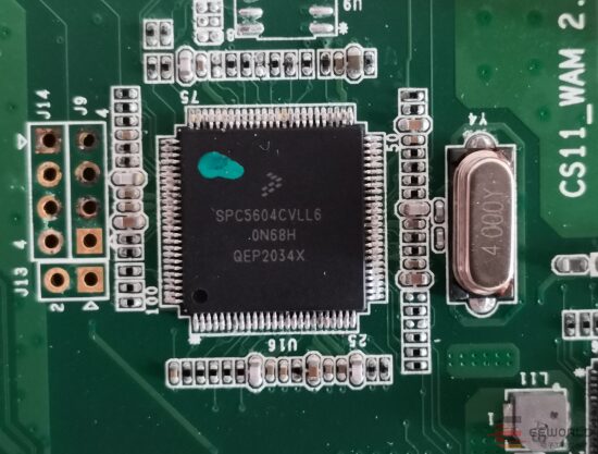
The coprocessor is SPC5604CAMLL6, a 32-bit microcontroller from NXP – MCU NXP 32-bit MCU, Power Arch core, 512KB Flash, 64MHz, -40/+125degC, Automotive Grade, QFP 100.
The display interface uses MAX9277GTM/V, Maxim’s 3.12Gbps GMSL Serializers for Coax or STP Output Drive and LVDS Input.
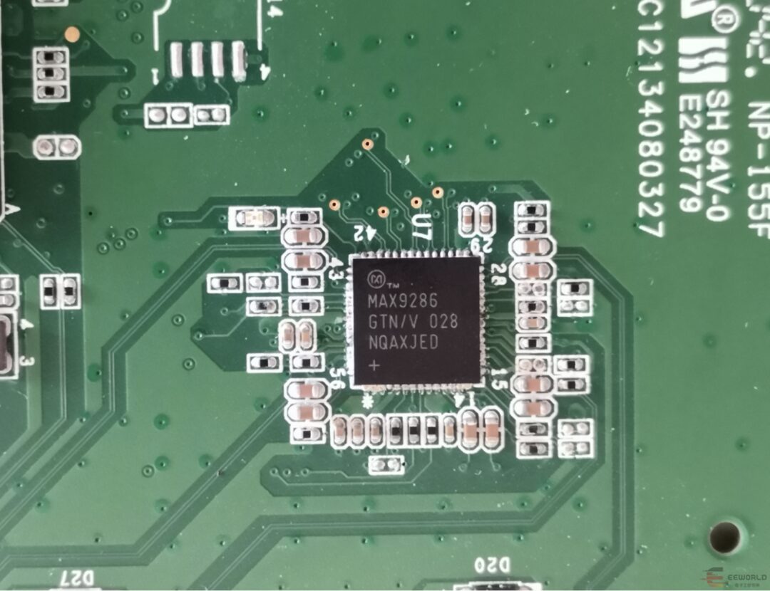
The camera data acquisition uses MAX9286GTN+, Maxim’s four-channel 1.5Gbps GMSL deserializer, with coaxial or STP input and CSI-2 output.
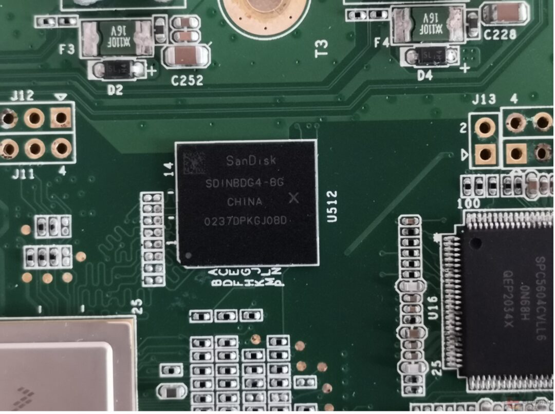
The flash memory is SDINBDG4-8G, SanDisk® iNAND® 7250 Industrial Embedded Flash Drives.
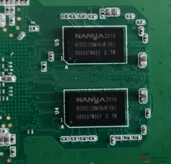
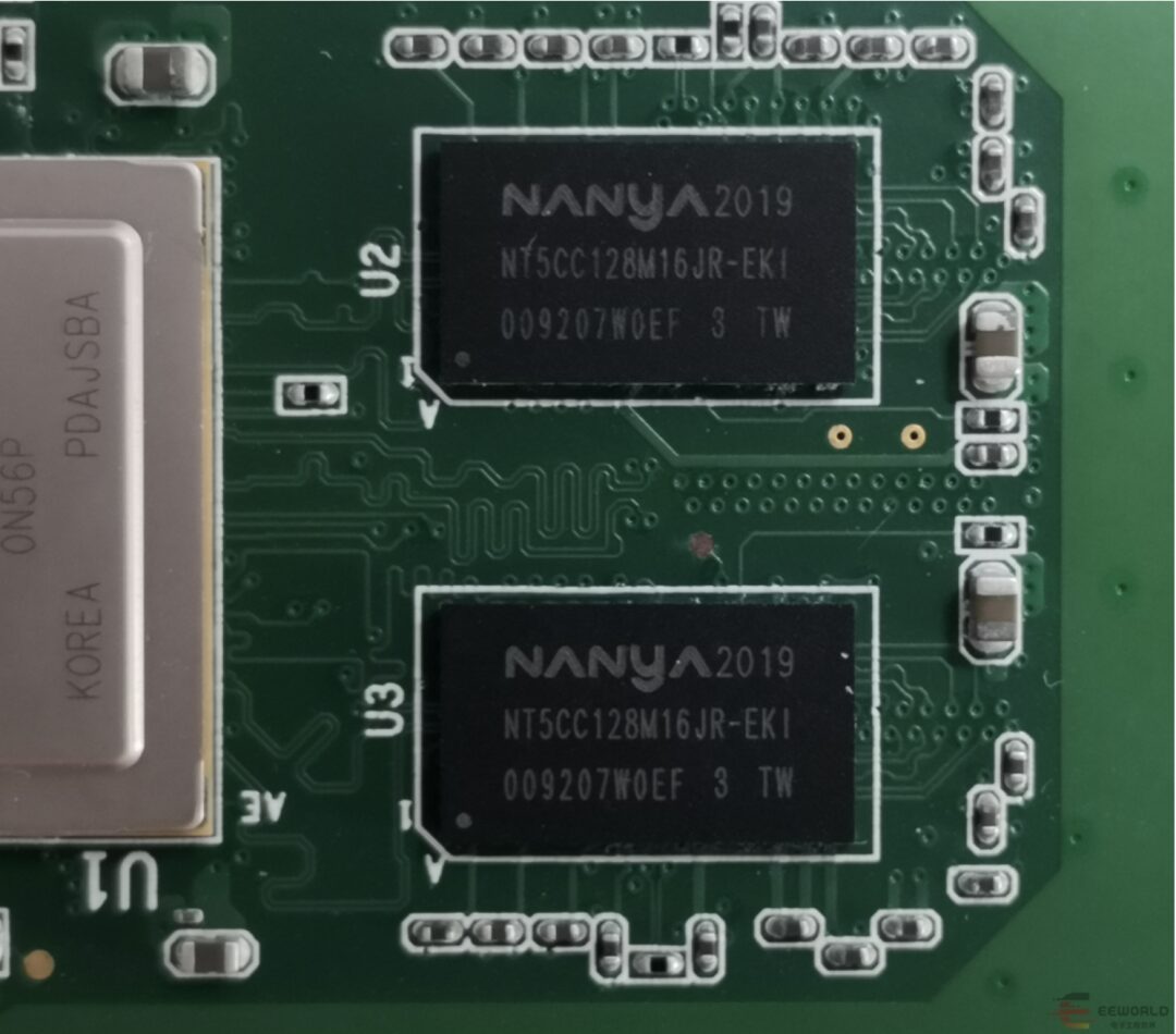
The memory consists of 4 pieces of Nanya’s NT5CC128M16JR-EK Commercial and Industrial DDR3(L) 2Gb SDRAM, totaling 8Gb.
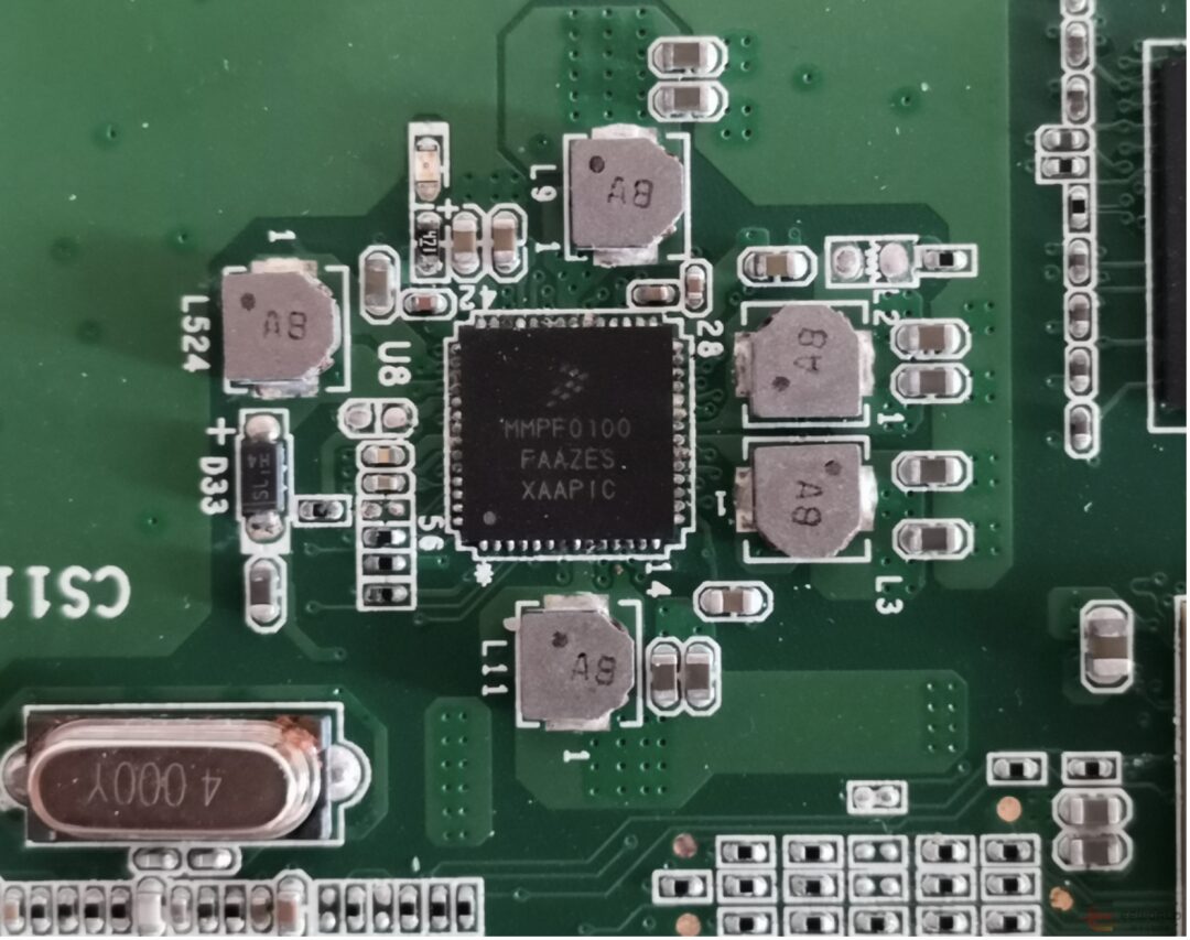
The power management chip is MMPF0100FAAZES, NXP’s 14 channel configurable power management integrated circuit.
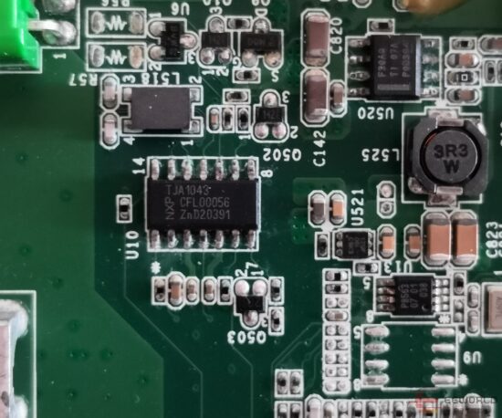
A TJA1043 NXP high-speed CAN transceiver is used for bus communication.
This chip is difficult to find, likely a PCF8563T NXP real-time clock ULTRA LOW PWR CLK/CAL RTC IC. It is unclear why the panoramic computer needs a real-time clock chip.
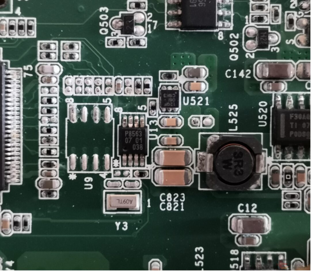
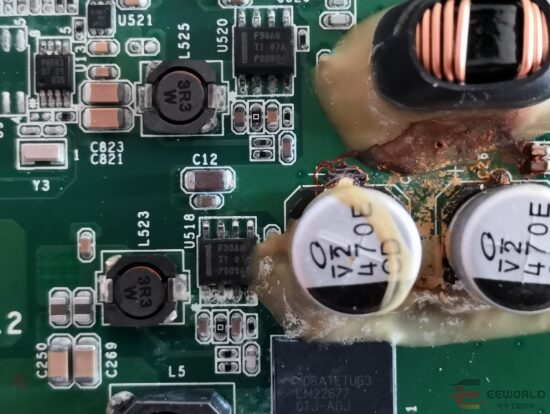
The main power uses two LMR23630AQDDAQ1 TI switch regulators, Automotive Qualified SIMPLE SWITCHER 4V to 36V, 3A Synchronous Step-Down Converter 8-SO PowerPAD -40 to 125.
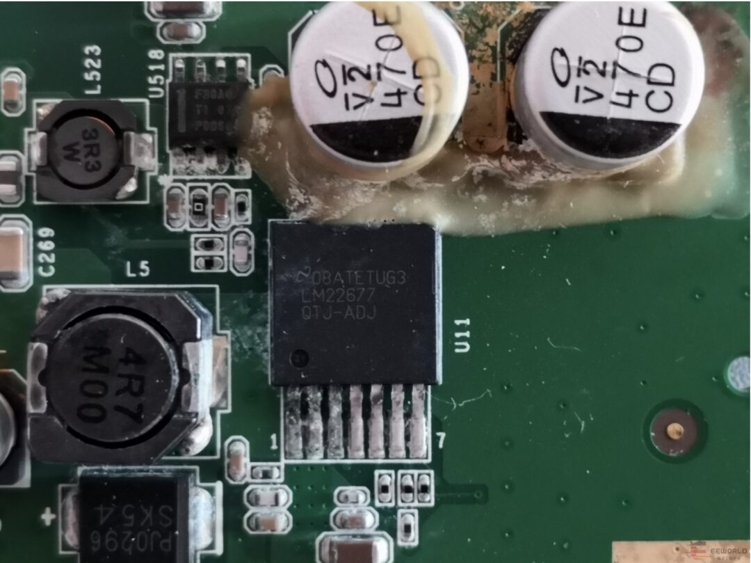
And an LM22677/-Q1 TI 42V, 5A SIMPLE SWITCHER® buck converter.
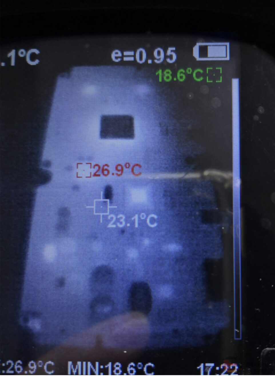
The overall craftsmanship is quite good, and the materials are quite solid. Finally, I supplied it with 12V using an adjustable power supply. I found that data output exists in some areas.
Using a multimeter to test the voltages of each power module should be normal. After working for a while, thermal imaging shows that the overall temperature rise is quite normal, indicating that most chips are functioning properly.
The screen output interface has no waveform; it is speculated that the i.MX 6 needs the coprocessor to receive instructions from the host before it can work.
The board is overall good except for slight corrosion on some components. It seems to be functioning normally, but it is unclear how to wake it up without the ECU. Now it is at least a potential i.MX 6 video development board.
As a vehicle safety configuration, the choice of chips and technical solutions inside the 360-degree imaging system undoubtedly arouses our strong interest. Today, we will disassemble a Lynk & Co brand 360-degree imaging computer to satisfy everyone’s curiosity about the secrets behind this technology.
This is a Lynk & Co 360 imaging computer that has been exposed to water, with most screws already removed by someone else.
After opening the shell, the internal rust is quite severe.
The board supports four camera inputs and one display output interface, using the NXP solution overall. After being washed with tap water, it looks quite nice.
The video processor is MCIMX6DP6AVT1AA, an NXP i.MX 6DualPlus Automotive Applications Processor.
The coprocessor is SPC5604CAMLL6, a 32-bit microcontroller from NXP – MCU NXP 32-bit MCU, Power Arch core, 512KB Flash, 64MHz, -40/+125degC, Automotive Grade, QFP 100.
The display interface uses MAX9277GTM/V, Maxim’s 3.12Gbps GMSL Serializers for Coax or STP Output Drive and LVDS Input.
The camera data acquisition uses MAX9286GTN+, Maxim’s four-channel 1.5Gbps GMSL deserializer, with coaxial or STP input and CSI-2 output.
The flash memory is SDINBDG4-8G, SanDisk® iNAND® 7250 Industrial Embedded Flash Drives.
The memory consists of 4 pieces of Nanya’s NT5CC128M16JR-EK Commercial and Industrial DDR3(L) 2Gb SDRAM, totaling 8Gb.
The power management chip is MMPF0100FAAZES, NXP’s 14 channel configurable power management integrated circuit.
A TJA1043 NXP high-speed CAN transceiver is used for bus communication.
This chip is difficult to find, likely a PCF8563T NXP real-time clock ULTRA LOW PWR CLK/CAL RTC IC. It is unclear why the panoramic computer needs a real-time clock chip.
The main power uses two LMR23630AQDDAQ1 TI switch regulators, Automotive Qualified SIMPLE SWITCHER 4V to 36V, 3A Synchronous Step-Down Converter 8-SO PowerPAD -40 to 125.
And an LM22677/-Q1 TI 42V, 5A SIMPLE SWITCHER® buck converter.
The overall craftsmanship is quite good, and the materials are quite solid. Finally, I supplied it with 12V using an adjustable power supply. I found that data output exists in some areas.
Using a multimeter to test the voltages of each power module should be normal. After working for a while, thermal imaging shows that the overall temperature rise is quite normal, indicating that most chips are functioning properly.
The screen output interface has no waveform; it is speculated that the i.MX 6 needs the coprocessor to receive instructions from the host before it can work.
The board is overall good except for slight corrosion on some components. It seems to be functioning normally, but it is unclear how to wake it up without the ECU. Now it is at least a potential i.MX 6 video development board.
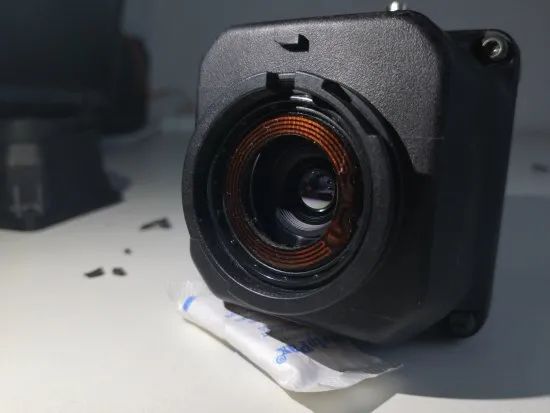
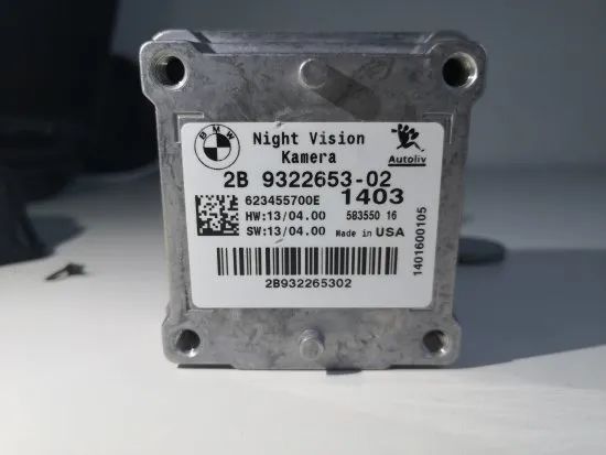
Disassembly of BMW Night Vision System: Infrared Camera
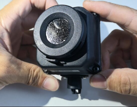
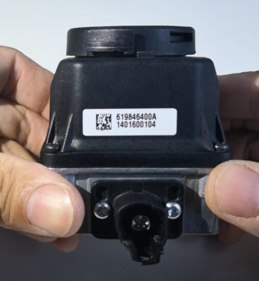
I bought several night vision cameras on a certain platform, this one is the NV3 version using a 4-pin HSD connector, slightly smaller than NV2. (For the specific disassembly process and high-definition images, please visit the forum: https://www.eeworld.com.cn/abrzDy1)
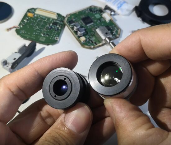
Removing the lens and protective lens reveals the heating coil inside, which has a 0603 thermal resistor that can be used to detect the temperature on the lens to determine whether to heat the lens.
After removing the back cover, the first thing I see is that the un-soldered pads on the power board are white, likely due to the use of silver plating. The pads in contact with the outer shell show severe oxidation, indicating that this camera has likely been exposed to moisture.
The back of the power board has fewer components, indicating that compared to NV2, the BOM cost has been significantly reduced.
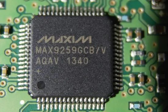
The main chips on the power board include a MAX9259GCB LVDS communication chip, which, when paired with MAX9260, can achieve 3.125Gbps data communication. The most remarkable feature is that it can also achieve low-speed bidirectional data communication like I2C or UART on two LVDS lines, making device interconnection more convenient.
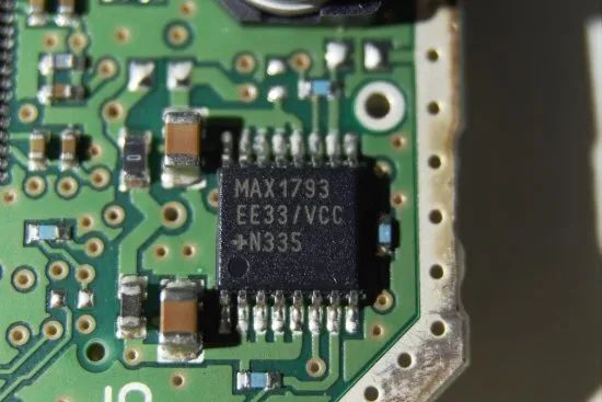
MAX1793EE33 is a 3.3V LDO that can provide 1A of current.
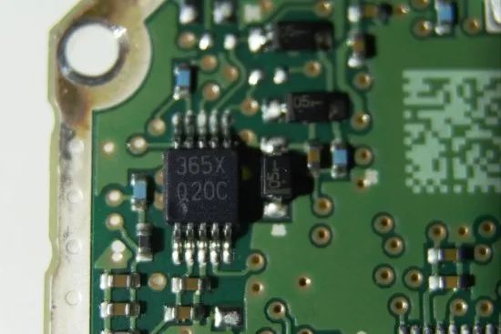
Silkscreen Q20C is TI’s ADC104S021Q, a 4-channel 10-bit ADC chip that supports sampling rates from 50K to 200KSPS.
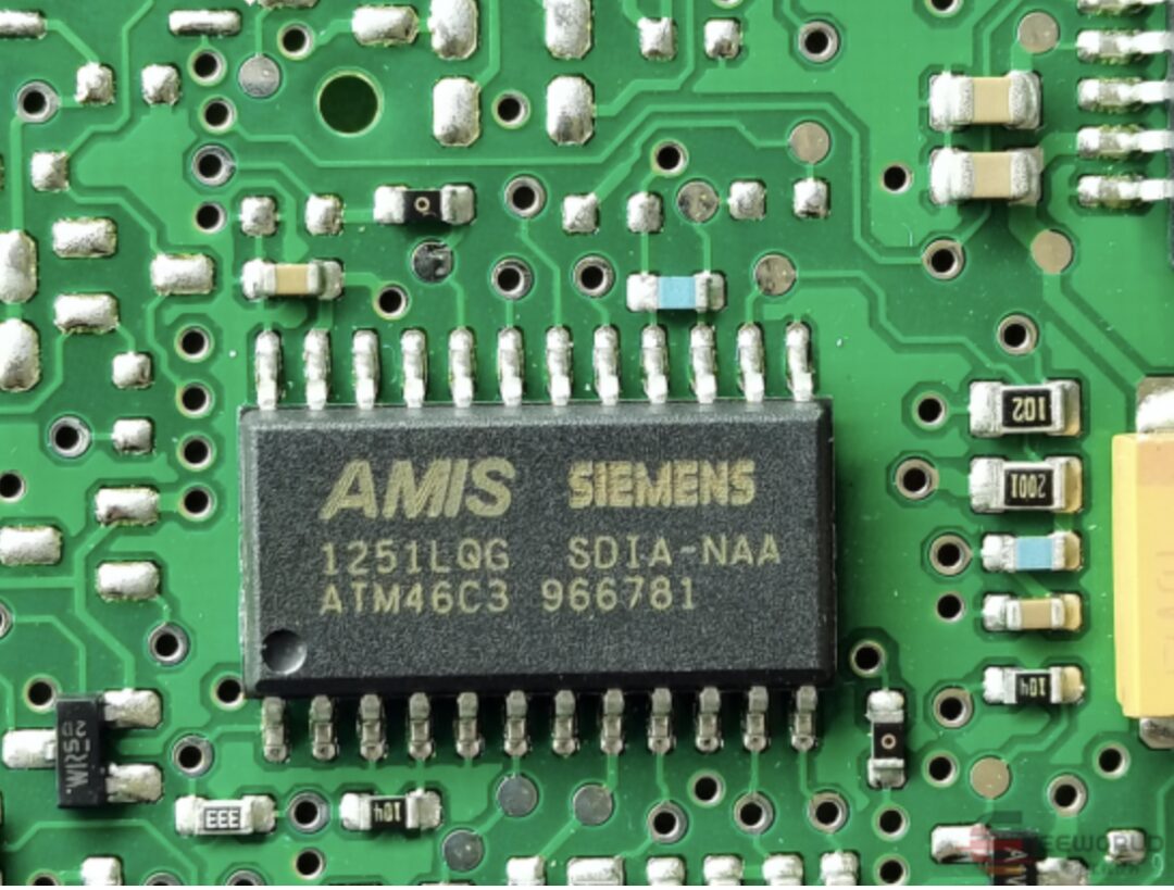
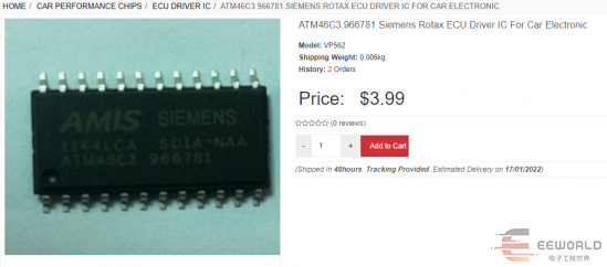
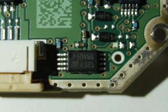
Silkscreen 504WG is ST’s 4KBit SPI interface EEPROM chip M95040.
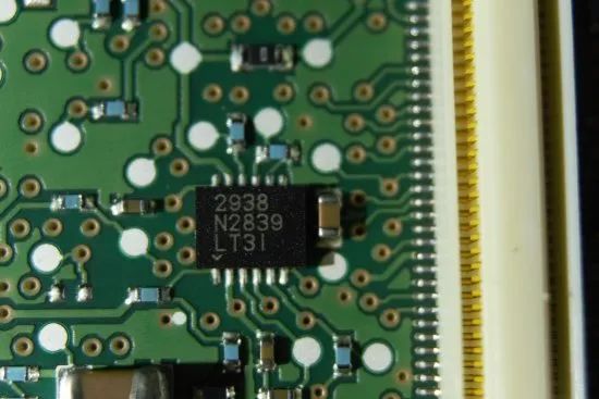
The back 2938 is ADI (Linear)’s LTC2938, a voltage monitoring chip.
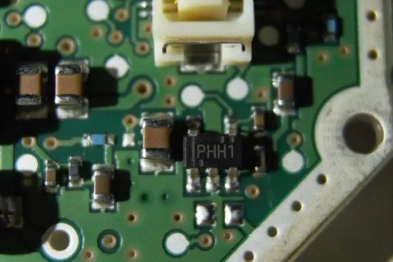
PHH1 is TI’s TPS79318, a 200mA 1.8V fixed output LDO.
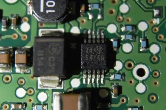
541GQ is TI’s TPS57140QDGQRQ1, a 3.5V~42V input, 1.5A Buck converter.
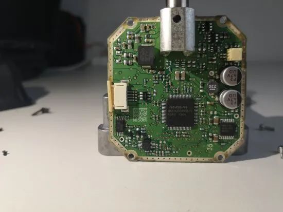
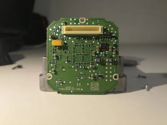
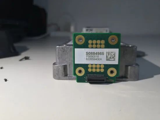
After removing the power board, there is also an FPGA core board inside, which includes FPGA, FLASH, DDR chips, and a MOLEX 40pin board-to-board connector for connecting to the sensor.
The back includes a DC-DC converter and a MOLEX 80pin board-to-board connector for connecting to the power board.
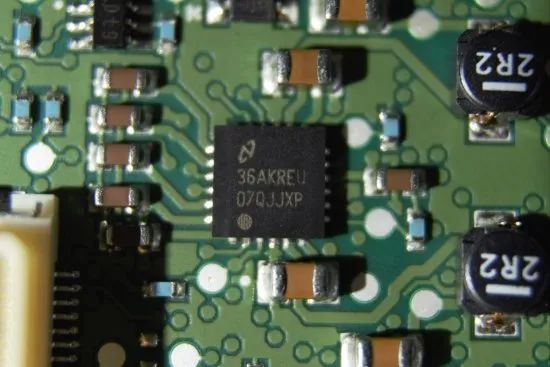
The back 07QJJXP is TI’s LP3907-Q1, a high-current I2C configurable buck converter, providing default outputs of 1.2 V and 3.3 V, plus 0.8 V and 2.5 V LDOs for a total of four outputs.
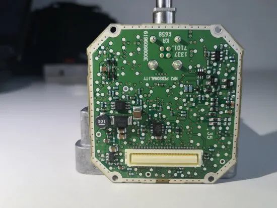
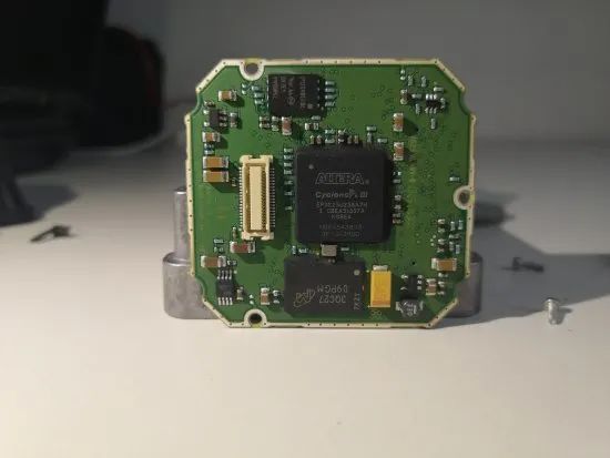
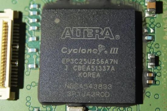
The front includes an EPS3C25U256A7N automotive-grade FPGA.
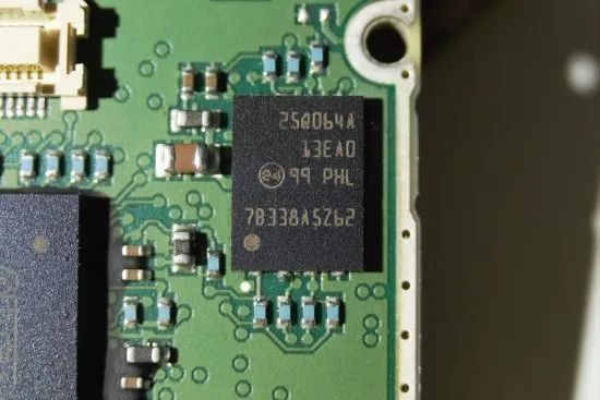
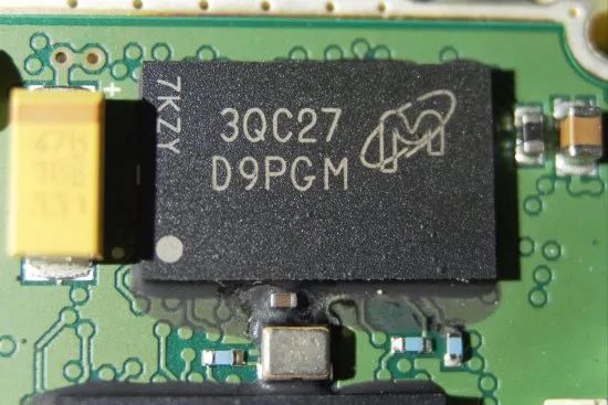
Silkscreen D9PGM is Micron’s 512M (16MX32) DDR memory.
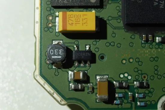
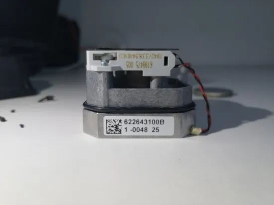
Silkscreen DCERZN is ON Semiconductor’s NCP1403, a boost converter.
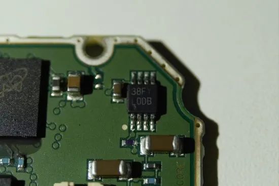
L0DB is TI’s LP2951-N, a 100mA LDO with an input range of 2.3 V~30 V.
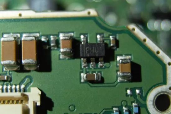
PHU1 is TI’s TPS79333DBVRQ1, a 200mA LDO.
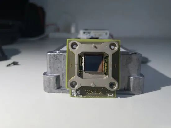
Removing the FPGA core board reveals the sensor beside it, FLIR ISC0901B0, a 17um 366*256 60fps 14-bit data output thermal imaging sensor.
Compared to NV2’s ISC0601, the size is smaller, and it looks simpler without a protective lens.
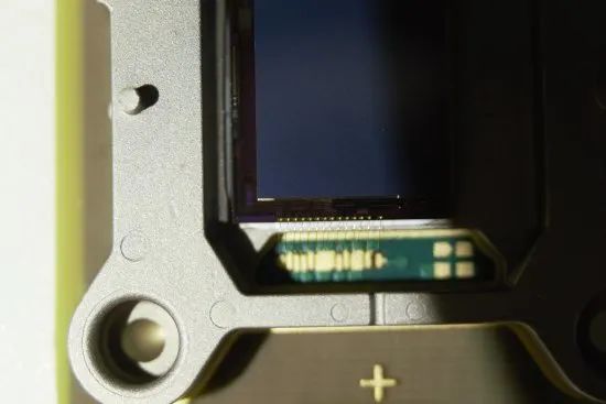
The gold wire on the side of the sensor is easily broken.
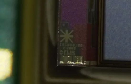
After magnifying, you can see the words FLIR ISC9001B0.
The shell bears the logos of BMW and Autoliv manufacturers.
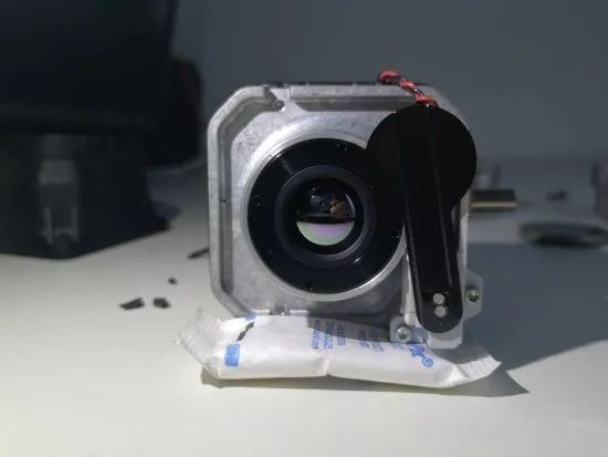
The shutter in front of the lens is used for flat field calibration and closes when powered on.
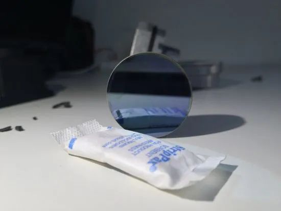
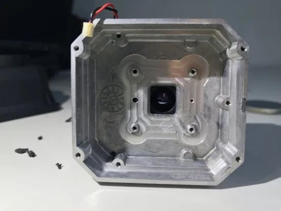
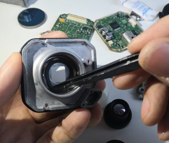
The internal lens image after removing the sensor.
The front image of the lens.
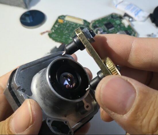
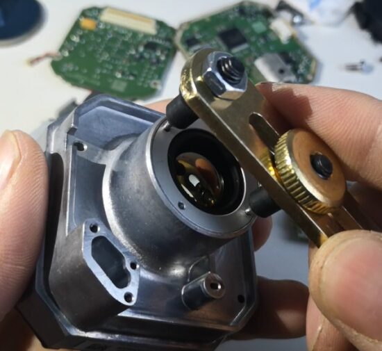
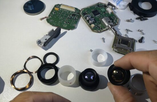
Removing the lens requires a “special” disassembly tool.
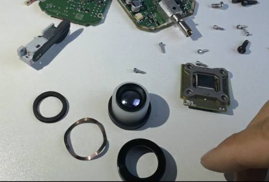
After removing the lens, there is also a metal spring and a thin film pad inside.
The lens assembly is much simpler compared to NV2’s camera.
NV3 has a black ring version and a white ring version.
The lens size of the white ring version is larger than that of the black ring version, and it has more components for installation and vibration reduction.
Now preparing to reverse the Altera board and then develop on it, as it has a considerable number of buses to communicate with the power board. I can draw a power board and use it to communicate with MAX9259GCB to drive an LCD or TF card. However, this seems quite difficult, and I probably won’t have time to do it. The next step is to add a collection board between the sensor and FPGA board to read the data directly and see.
█ Final Words
A person can go fast, but a group can go further.Xiaoxin’s Knowledge Circle has over 250 members already. If you also need a good learning environment,click the link 🔗 to join us. This is a hardware learning guide + project practice + interview coaching private circle where you can read the top posts, ask questions, help you formulate learning plans, and grow together with friends.
The circle has already purchased many materials and books, all of which will be filtered by me and then recommended to everyone. This investment is definitely worth it! Less than 1 yuan a day!
Currently, the top post has accumulated a lot of high-quality learning resources, which I believe can help you go faster, more steadily, and further!