 2025/03/22, Advanced Photonics
Based on AMF’s latest Process Design Kit (PDK4.5) PESiN-on-SOI wafer fabrication process (process capabilities are backward compatible), Xiaoguang regularly organizes silicon-based photonic chip wafer fabrication services, providing a full-process solution from design to delivery:
1) Design Services: Photonic integrated components, system simulation, and design;
2) Layout Services: Layout drawing and review in conjunction with PDK;
3) Wafer Fabrication Services: Layout integration, DRC, and wafer processing;
4) Packaging and Testing Services: Including optical and electrical packaging tests at the device and module levels.
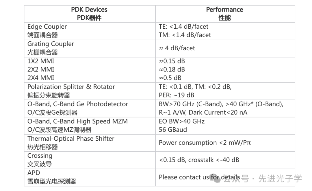
Main Highlights of AMF’s Latest Process Design Kit (PDK4.5)
30% efficiency improvement with a new type of modulator
High-speed photodetector (90GHz)
Compact 80GBaud photodetector
High-speed micro-ring modulator (70GHz)
Avalanche photodetector (APD)
2D Optical Phased Array (OPA)
Si Grating Coupler
Flexible Services and Technical Support
Since 2003, AMF has been a leading supplier in integrated photonic technology with strong delivery capabilities. Through the latest upgraded ultra-clean factory and chip manufacturing equipment, AMF can provide short wafer fabrication cycles, high quality, and high reliability services for various users.
* Multi-project wafer fabrication (MPW) and custom services for proof of concept
* Small-scale production services for product validation
* Large-scale production services for commercial product applications
Silicon-based Photonic Device Model Library
Wafer Fabrication Service Process Features
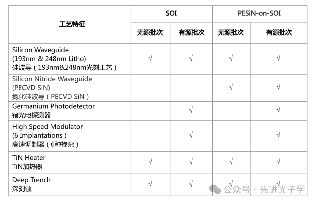
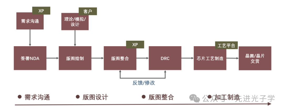
Figure 1. Full process from design to delivery
For more details on customized wafer fabrication services, please contact:
Sales Contact: Xiaoguang
Sales Phone: 18811555924
Email: [email protected]
AMF | Advanced Micro FoundryAMF is spun off from the Singapore A*STAR Institute of Microelectronics (IME) and is a world-leading commercial silicon-based photonic process line that supports customers in achieving “concept-prototype-mass production” wafer fabrication models. AMF’s professional team consists of experts in optics and semiconductors, capable of closely collaborating with user teams to ensure the realization of silicon-based photonic chips for various applications.https://www.advmf.com/ X PHOTONICS
X PHOTONICS focuses on the field of optoelectronic integration technology. It provides Chinese users with optoelectronic integrated layout implementation services, optoelectronic hybrid packaging testing equipment and services, SOI/Si3N4/SiO2 wafer fabrication services, etc. Technical cooperation involves silicon photonic communication optical modules, integrated LiDAR modules, integrated optical frequency comb chips, and integrated optical quantum information chips.

Advanced Photonics
“Advanced Photonics” is a media outlet in the field of optoelectronics, focusing on the stage of technology research being transformed into mass-produced products. It introduces technologies and products with batch application prospects, publishes market analysis reports, compiles information on industry exhibitions, industrial forums, and technical exchange meetings, and selects books and materials related to market hotspots.
 Advanced Photonics WeChat Subscription Account
Advanced Photonics WeChat Personal Account
Xiaoguang 18811555924 (same number for WeChat)
Copyright StatementThis article’s copyright belongs to the original author and the information provider. If the content of the article involves copyright and other issues, please contact the above phone number or WeChat immediately.