Source: Semiconductor Industry Overview
Original Author: Feng Ning
Traditional chip architectures face severe challenges such as the “memory wall,” “power wall,” and “compute wall.” What are they? What is a unified memory-compute chip? How does it solve these problems?
In recent years, with the explosive growth of AI application scenarios, the demand for computational power by AI algorithms has surged sharply, significantly outpacing the hardware performance improvement speed predicted by Moore’s Law. Traditional computing chips are gradually revealing limitations in meeting the high parallel computing demands of AI in terms of computing resources, processing delay, and power consumption control.
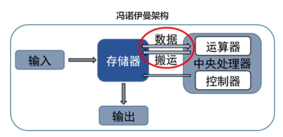
In the field of smart chips, the traditional von Neumann architecture focuses on computation, and the physical separation between processors and memory leads to frequent data migrations, further limiting the overall performance of AI chips. Therefore, traditional chip architectures face severe challenges such as the “memory wall,” “power wall,” and “compute wall,” making it difficult to meet the urgent demands of AI applications for low latency, high energy efficiency, and high scalability.
To address these issues, the industry has proposed a solution known as “unified memory-compute.”
Three Walls Facing Chip Development
First, let’s understand what the “memory wall” is.
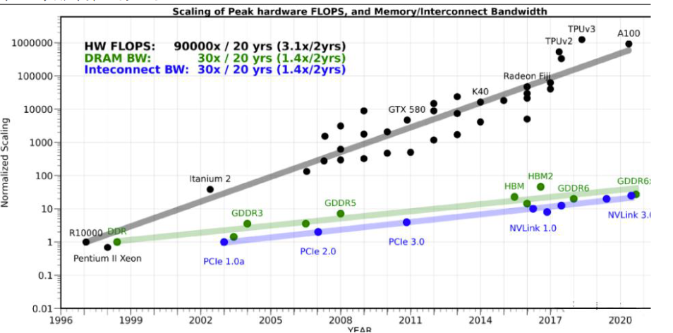
The memory wall refers to the phenomenon where memory performance severely limits CPU performance. Over the past 20 years, processor performance has rapidly increased at a rate of about 55% per year, while memory performance has only improved at around 10% per year. This long-term unbalanced development has led to the current memory access speed lagging significantly behind the computational speed of processors, creating a bottleneck that severely restricts the efficacy of high-performance processors and greatly constraining the growing demand for high-performance computing. This serious memory bottleneck that hinders processor performance is called the “memory wall.”
 Storage-Compute “Scissors Gap” Source: OneFlow Company, Anxin Securities Research Center
Accompanying the “memory wall” issue is the significant energy consumption incurred during data transmission, leading to a marked reduction in the energy efficiency of chips, known as the “power wall” issue.
The “power wall” issue mainly arises from the continuous increase in memory bandwidth demands of computing systems and the pursuit of higher capacity and faster access speeds, causing the power consumption of traditional DRAM and other types of memory to surge dramatically, ultimately reaching a critical point that cannot be resolved by simply increasing the power budget.
This is partly because data moving from DRAM to CPU has to traverse multiple levels of storage hierarchy, including L1, L2, and L3 caches. Research shows that, under certain conditions, the energy consumed to move 1 bit of data from DRAM to CPU can be several times to dozens of times higher than the energy required to process that bit on the CPU.
According to Intel’s research, when semiconductor processes reach 7nm, the data transport power consumption can reach as high as 35pJ/bit, accounting for 63.7% of total power consumption. The power loss caused by data transmission is becoming increasingly severe, limiting the speed and efficiency of chip development.
The “compile wall” issue is hidden between the two, where the large amount of data transport in a very short time prevents the compiler from optimizing operators, functions, programs, or networks as a whole in a statically predictable manner, and manual optimization consumes a lot of time.
In the past, the rapid improvement of computational power could still compensate for the drawbacks of these three “mountains” due to advanced processes.
But a harsh reality is that the old method of improving chip computational power through process technology over the past decades is gradually failing—Moore’s Law is approaching its physical limits, traditional “solutions” like HBM, 3D DRAM, and better interconnects only address symptoms without solving the root cause, and the miniaturization of transistors is becoming increasingly difficult, making it harder to improve computational performance while reducing power consumption.
With the arrival of the large model era, the surge in data computation has undoubtedly amplified the impact of the “three walls.”
The emergence of unified memory-compute technology is a powerful response to these challenges.
Storage-Compute “Scissors Gap” Source: OneFlow Company, Anxin Securities Research Center
Accompanying the “memory wall” issue is the significant energy consumption incurred during data transmission, leading to a marked reduction in the energy efficiency of chips, known as the “power wall” issue.
The “power wall” issue mainly arises from the continuous increase in memory bandwidth demands of computing systems and the pursuit of higher capacity and faster access speeds, causing the power consumption of traditional DRAM and other types of memory to surge dramatically, ultimately reaching a critical point that cannot be resolved by simply increasing the power budget.
This is partly because data moving from DRAM to CPU has to traverse multiple levels of storage hierarchy, including L1, L2, and L3 caches. Research shows that, under certain conditions, the energy consumed to move 1 bit of data from DRAM to CPU can be several times to dozens of times higher than the energy required to process that bit on the CPU.
According to Intel’s research, when semiconductor processes reach 7nm, the data transport power consumption can reach as high as 35pJ/bit, accounting for 63.7% of total power consumption. The power loss caused by data transmission is becoming increasingly severe, limiting the speed and efficiency of chip development.
The “compile wall” issue is hidden between the two, where the large amount of data transport in a very short time prevents the compiler from optimizing operators, functions, programs, or networks as a whole in a statically predictable manner, and manual optimization consumes a lot of time.
In the past, the rapid improvement of computational power could still compensate for the drawbacks of these three “mountains” due to advanced processes.
But a harsh reality is that the old method of improving chip computational power through process technology over the past decades is gradually failing—Moore’s Law is approaching its physical limits, traditional “solutions” like HBM, 3D DRAM, and better interconnects only address symptoms without solving the root cause, and the miniaturization of transistors is becoming increasingly difficult, making it harder to improve computational performance while reducing power consumption.
With the arrival of the large model era, the surge in data computation has undoubtedly amplified the impact of the “three walls.”
The emergence of unified memory-compute technology is a powerful response to these challenges.
What Surprises Does Unified Memory-Compute Bring?
From the principle of unified memory-compute technology, the core of unified memory-compute is to integrate storage and computation functions on the same chip, directly using storage units for data processing—by modifying the “read” circuit of the in-memory computing architecture, computation results can be obtained in the “read” circuit and written back directly to the target address in memory, eliminating the need for frequent data transfers between computation and storage units, significantly reducing power consumption and greatly enhancing computational efficiency.
As a result, unified memory-compute technology can effectively overcome the bottlenecks of the von Neumann architecture.
So, what performance improvements can unified memory-compute technology bring in practical applications due to its technical advantages?
Unified memory-compute chips can provide greater computational power (over 1000 TOPS) and higher energy efficiency (over 10-100 TOPS/W) in specific fields, significantly surpassing existing ASIC computational power chips. Unified memory-compute technology can also enhance computational power by utilizing storage units for logical computations, which is equivalent to scaling up the number of computation cores without changing the area.
In terms of energy consumption control, unified memory-compute technology can reduce energy consumption to 1/10 to 1/100 of previous levels by minimizing unnecessary data transport. By improving computational efficiency and reducing power consumption, unified memory-compute naturally brings better cost returns.
Classification of Unified Memory-Compute Technology
Based on the distance between storage and computation, the broadly defined unified memory-compute technology can be divided into three categories: Processing Near Memory (PNM), Processing In Memory (PIM), and Computing In Memory (CIM).
Processing Near Memory is a relatively mature technical path. It utilizes advanced packaging technology to package computation logic chips and memory together, achieving high I/O density by reducing the distance between memory and processing units, thus achieving high memory bandwidth and lower access overhead. Processing Near Memory is mainly achieved through 2.5D and 3D stacking technologies and is widely used in various CPUs and GPUs.
Processing In Memory primarily focuses on embedding the computation process as much as possible within the memory itself. This implementation aims to reduce the frequency of processor access to memory since most computations are already completed within the memory. This design helps eliminate the issues caused by the von Neumann bottleneck, improving data processing speed and efficiency.
Computing In Memory also integrates computation and storage into one technology. It has two main approaches. The first approach involves circuit innovations that give memory itself computational capabilities. This typically requires modifications to SRAM or MRAM to implement computational functions in places like the data readout decoder. This method usually has a higher energy efficiency ratio, but the computational accuracy may be limited.
Among these, Processing Near Memory and Computing In Memory are currently the mainstream paths for implementing unified memory-compute technology.
Main Choices of Storage Media
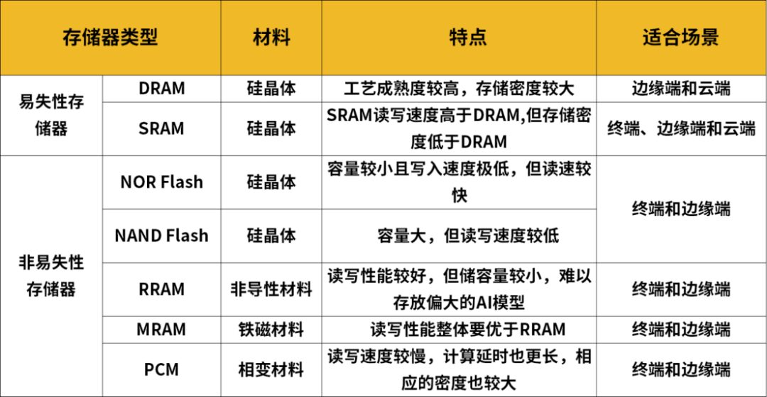
The storage media for unified memory-compute chips can be divided into two main categories: one is volatile memory, which loses data when the system is normally shut down or unexpectedly closed, such as SRAM and DRAM.
The other is non-volatile memory, which does not lose data under the above circumstances, such as traditional flash memory NOR Flash and NAND Flash, as well as new types of memory: Resistive Random Access Memory (ReRAM), Magnetic Random Access Memory (MRAM), Ferroelectric Random Access Memory (FeRAM), and Phase Change Memory (PCM).
So, how should we choose the appropriate technical path, and what characteristics, barriers, and advantages do these technical paths have?
From the perspective of device process maturity, SRAM, DRAM, and Flash are all mature storage technologies.
Flash is a non-volatile memory device with a low-cost advantage, generally suitable for low computational power scenarios; DRAM is low-cost with large capacity, but the available eDRAM IP core process nodes are not advanced, reading latency is also large, and it requires periodic data refresh; SRAM has a significant speed advantage, almost the highest energy efficiency ratio, with slightly smaller capacity density, and can ensure high accuracy after precision enhancement, generally suitable for cloud computing and other high computational power scenarios.
In terms of process technology, SRAM can be manufactured on advanced processes such as 5nm, while DRAM and Flash can be manufactured on 10-20nm processes.
In terms of circuit design difficulty, In-Memory Computing DRAM > In-Memory Computing SRAM > In-Memory Computing Flash. In In-Memory Computing, SRAM and DRAM are more difficult to design since they are volatile memories, and process deviations significantly increase the design difficulty of analog computing. Flash is a non-volatile memory, and its state is continuously programmable, allowing for calibration of process deviations through programming, thus improving accuracy. Processing Near Memory designs are relatively simple and can use mature storage technology and logic circuit design techniques.
In addition to mature storage technologies, academia is also paying attention to the introduction of various RRAM in neural network computing. RRAM uses resistance modulation to achieve data storage and reads out current signals instead of traditional charge signals, which can provide better linear resistance characteristics. However, the yield rate of RRAM processes is still climbing, and it still faces inherent reliability issues of non-volatile memory, so it is currently mainly used for edge AI computing and small computational power scenarios.
Applicable Scenarios for Unified Memory-Compute Chips
Low Computational Power Scenarios: Edge applications are very sensitive to cost, power consumption, latency, and development difficulty
In the early stages, unified memory-compute chips had relatively low computational power, starting from 1 TOPS, addressing audio, health, and low-power visual terminal applications, as well as the performance and power consumption issues of AI chips. For example: AIoT (Artificial Intelligence of Things) applications.
It is well-known that the fragmented AIoT market does not have a strong demand for advanced process chips, but instead prefers low-cost, low-power, and easy-to-develop chips.
Unified memory-compute chips are precisely in line with these requirements.
Firstly, unified memory-compute technology can significantly reduce energy consumption by minimizing data movement between storage and computation units. For example, in traditional architectures, massive data transfers consume a lot of energy, while unified memory-compute architectures can avoid this unnecessary energy consumption, enabling battery-powered IoT devices to operate for longer periods.
Secondly, by reducing data transmissions and improving integration, unified memory-compute technology can lower manufacturing costs for chips. For large-scale deployments of AIoT devices, cost reductions facilitate wider application promotion.
Finally, unified memory-compute chips can greatly enhance computation speed and save space, which are two major factors that support AIoT applications.
High Computational Power Scenarios: GPUs cannot compete with dedicated acceleration chips in both computational power and energy efficiency
Currently, the cloud computing computational power market, the single architecture of GPUs can no longer adapt to the discrete algorithm characteristics of different AI computing scenarios, such as mainstream algorithm architectures in image, recommendation, and NLP fields.
As unified memory-compute chip computational power continues to rise, its application range is gradually expanding into high computational power application fields. For high computational power scenarios >100 TOPS, it provides high-performance, cost-effective products for autonomous vehicles, general robotics, intelligent driving, and cloud computing.
Additionally, unified memory-compute chips have other extended applications, such as sensing-compute integration and brain-like computing.
The moment when unified memory-compute chips are widely implemented is still uncertain, but the arrival of that day is worth looking forward to. The evolution of technology never stops, and market demands are constantly changing. When various conditions mature, it may be the time for unified memory-compute chips to shine.
END
Reprinted content only represents the author’s views
It does not represent the position of the Semiconductor Institute of the Chinese Academy of Sciences
Editor: March
Editorial Supervisor: Mu Xin
Submission Email: [email protected]
1. Significant progress in bionic covering neuron model and learning methods at the Semiconductor Institute
2. Important progress in inverted structure perovskite solar cells at the Semiconductor Institute
3. Why do chips use copper as interconnect metal?
4. What exactly is the 7nm of chips?
5. Silicon-based integrated optical quantum chip technology
6. How unusual is the quantum anomalous Hall effect? It may lead to the next revolution in information technology!