Hard Switch Circuit Design Example
The hard switch circuit converts the series voltage of two 7-cell batteries into a 3.3 V voltage through the DC/DC converter MAX756, as shown in Figure 1. If powered directly by the batteries without a boost circuit, the voltage at the battery terminal will experience a decline from high to low. The series voltage of two new batteries is above 3 V; as energy is depleted, it will drop below 2V, causing the machine to malfunction. The JM2 button serves as the power on/off switch. When the JM2 button is pressed, contact bounce may cause misoperation. The charging and discharging circuit formed by R20, C13, R21, R22, R23, and V9 is designed to eliminate button bounce by appropriately selecting the values of R20, C13, and R21, ensuring that both the charging and discharging times of the circuit exceed the button bounce time. The key pulse output from the collector of V9 is debounced and then further filtered and shaped by U25 (74HC14), which consists of three inverters with Schmitt triggers, generating a complete single pulse. This pulse triggers the flip-flop of U24A (74HC74 D flip-flop).
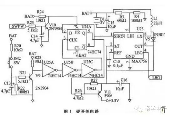
In Figure 1:
① If the Q output of U24A pin 5 is high, then the Q output of pin 6 is low, and this low input is sent to the inhibit pin (pin 1) of MAX756 (active low). At this time, MAX756 is in the off state, but due to the presence of the pulse rectifier V5 in the DC/DC conversion circuit, the battery voltage still reaches the output pin 6 of DC/DC through V5. Therefore, a transistor V11 must be added to the circuit as a switching element. When the Q output of pin 6 of U24A is low, putting MAX756 in the inhibit state, the Q output of pin 5 of U24A is high, causing transistor V11 to be in the cutoff state, thus completely shutting off the path from the battery to the main circuit power VCC, putting the machine in the off state, with the entire machine current measured to be no more than 5uA.
② When the button pulse triggers the flip-flop of U24A (74HC74 D flip-flop), the Q output of pin 5 of U24A goes low and the Q output of pin 6 goes high, putting MAX756 in the working state, as the control pin 2 for output voltage is high, resulting in an output of +3.3 V. At the same time, the low output from pin 5 of U24A turns on transistor V11, allowing MAX756 to provide working power to the main circuit, thus the machine is powered on.
In the powered-on state, the output SWPW of the microcontroller remains low. When the microcontroller changes the SWPW output to high, the inverting circuit formed by V10 outputs a low signal, making pin 1 of U24A effective, with the Q output of pin 5 going high and pin 6 going low, thus shutting down the machine. Therefore, SWPW can serve as the “automatic shutdown” signal. Due to the high output of the I/O port during the microcontroller’s power-on reset, the high SWPW during reset may cause a “reset mis-shutdown” phenomenon. To prevent this from occurring, a charging circuit formed by R25 and C14 is added to the SWPW output circuit. By appropriately selecting the values of R25 and C14, SWPW can be kept low before the charging circuit reaches the threshold voltage of 0.7 V for V10 after reset, thus avoiding the “reset mis-shutdown” phenomenon.
The LBI pin (pin 5) of MAX756 is used to detect low battery voltage. If the voltage on this pin drops below the internal reference voltage of 1.25 V, the LBO pin (pin 4, open-drain output) of MAX756 will output a low signal, which can serve as a low battery alarm signal. There are two bases for setting the alarm voltage point.
① The national standard requires the battery termination voltage to be 0.9 V. After actual measurement, when the series voltage of two 7-cell batteries drops below 2V, the battery energy is nearly depleted and can no longer maintain stable operation of the product. Therefore, the low voltage detection alarm point is set at 2 V.
The reason this circuit is called a hard switch circuit is mainly because pressing JM2 can achieve power on/off without requiring assistance from the microcontroller. The role of SWPW is to enable timed automatic shutdown. The next battery-powered circuit discussed requires the microcontroller to assist in controlling the power on/off.
Soft Switch Circuit Design Example
In the power management circuit shown in Figure 2, the RN5RK331A DC/DC converter from Ricoh is used to convert the voltage provided by the battery into a 3.3 V voltage to supply the main circuit, ensuring that the machine can operate stably throughout the battery life cycle.
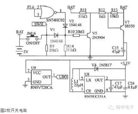
The process of turning the machine on/off in this circuit can be divided into two cases:
① In the off state, the JM16 key is used as the power on button. Pressing JM16 causes the battery voltage to reach the base of V5 through V1, turning on V5 and V7; the battery voltage then reaches the input and enable pins of the DC/DC converter RN5RK331A, causing it to start working and output 3.3 V power to the main circuit. After the payment password device is powered on, the microcontroller outputs a low signal from P3.6, which is inverted and then keeps V5 and V7 in the on state through V2. This way, even after releasing the JM16 key, the payment password device can remain powered on, with the low output from P3.6 serving to maintain the power on state.
② In the powered-on state, the JM16 key is used as the power off button. When the JM16 key is not pressed, the SWH signal point is low. Pressing the JM16 key raises the SWH signal point to high; this signal change is read by the microcontroller through the keyboard interface. When the closure of JM16 is detected during power on, it is recognized as a shutdown command. After the JM16 key is released, the microcontroller outputs a high signal from P3.6, which is inverted and then turns off V5 and V7 through V2, causing the payment password device to shut down due to lack of power supply. In this power supply circuit, the transistor V7 acts as the switch element for battery power and is placed in front of the DC/DC converter circuit. During shutdown, it completely cuts off the power supply circuit of the DC/DC converter, further reducing the leakage current during shutdown. After the whole machine is powered off, it is detected that the shutdown current is less than 5uA. The low battery voltage detection alarm in Figure 2 is implemented by the RN5VT20CA (U9) from Ricoh, with a fixed detection voltage of 2V.
Compared to Figure 1, after powering on with the JM16 key, it is necessary to utilize the low output from the microcontroller P3.6 to maintain the power on state, hence this circuit is called a “soft switch circuit.” The advantage of using this soft switch circuit is that there is no need to consider button debounce issues, the hardware circuit is simple, which can lower hardware costs and save PCB space; in handheld products, PCB space is very valuable (the number of components directly affects the size of the PCB and the overall appearance of the product). The disadvantage is that when subjected to strong external signal interference or if the battery power is insufficient, the JM16 button may not function, requiring the battery to be removed and reinserted to resolve the freeze issue. Of course, the probability of this occurring is very low, and when the freeze is caused by insufficient battery power, the battery needs to be replaced. In contrast, in the hard switch circuit of Figure 1, when encountering a freeze issue, it is not necessary to touch the battery; the machine can be powered on and off by pressing the JM2 button.
Power Supply Filtering
In the DC/DC conversion circuit described above, a boost converter device is used, and the circuit structure of the boost-type DC/DC converter is shown in Figure 3.
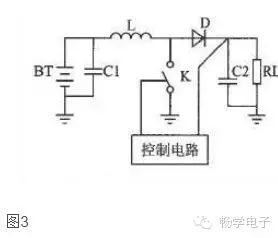
When the switch K is closed, the battery BT charges the inductor L, storing energy in the form of a field 1/(2L×I2). Here, I is the inductor current. When K is opened, the magnetic energy in L is released to the filter capacitor C2 and load RL in the form of electrical energy. Periodic switching operations continuously supply energy from the battery to the load, while the output voltage is converted to:
Vout = Vin/(1-δ)
where δ is the duty cycle (the ratio of the on time to the working cycle). The control circuit monitors the output voltage and controls the duty cycle to adjust and stabilize the output voltage. The control method of the DC/DC boost converter described in this article is PFM (Pulse Frequency Modulation), which has a lower static current and higher efficiency under light load conditions, but slightly higher ripple. To ensure stable operation of the main circuit, filtering of the power supply output must be considered. Generally, passive filtering circuits are used, with the main forms being capacitive filtering, inductive filtering, and composite filtering (including inverted L-type, LCπ-type filtering, and RCπ-type filtering, etc.). When using inductive filtering or composite inductive filtering, a large inductance value is required, which is not suitable for handheld or portable products. Therefore, in cases of small load current, RCπ-type filtering is used, which is simple in structure, economical, and provides good filtering effect. The equivalent series resistance (ESR) of the filter capacitor is the main factor causing output ripple, and the capacitor material should be chosen to have a lower ESR, such as ceramic capacitors, aluminum electrolytic capacitors, and tantalum electrolytic capacitors, while standard aluminum electrolytic capacitors should be avoided. When using RCπ-type filtering, the ripple coefficient S across the output voltage is given by S=1/(Kω×C×R). K is a constant, and from this formula, it can be seen that for a given ω value, the larger the R and C, the smaller the ripple coefficient, meaning better filtering effect. However, increasing R will also increase the DC voltage drop across the resistor, thus increasing the internal loss of the DC power supply; increasing the capacitance of C will also increase the size and weight of the capacitor, making it difficult to achieve. Therefore, the capacitance is generally set between 10-100 uF, and the resistance value is generally below 10Ω.
Conclusion
The two battery-powered circuits introduced above convert the battery voltage into +3.3 V DC voltage, providing a working power supply for microcontroller application systems through DC/DC boost circuits. These circuits are mainly used in products powered by two 7-cell batteries, such as PDAs and handheld terminals. Other products (such as mobile phones and digital cameras) may have different battery power supply circuits, but the working principles are generally similar. In the design of battery-powered circuits, a series of issues need to be addressed, such as how to implement power on/off, reduce shutdown current, minimize ripple and interference signals in the output power supply, and improve conversion efficiency. Only by properly solving these problems can the product operate stably and reliably. The two examples discussed in this article effectively address these issues and have been successfully applied in products with good results. Of course, with the continuous emergence of new devices, the design of such circuits needs to be continuously improved and refined to enhance the overall performance of the product.