In Buck-type DC-DC power circuits, the PCB layout is crucial for the implementation of circuit functionality and achieving good performance metrics.
Key Layout Considerations for Current Loops
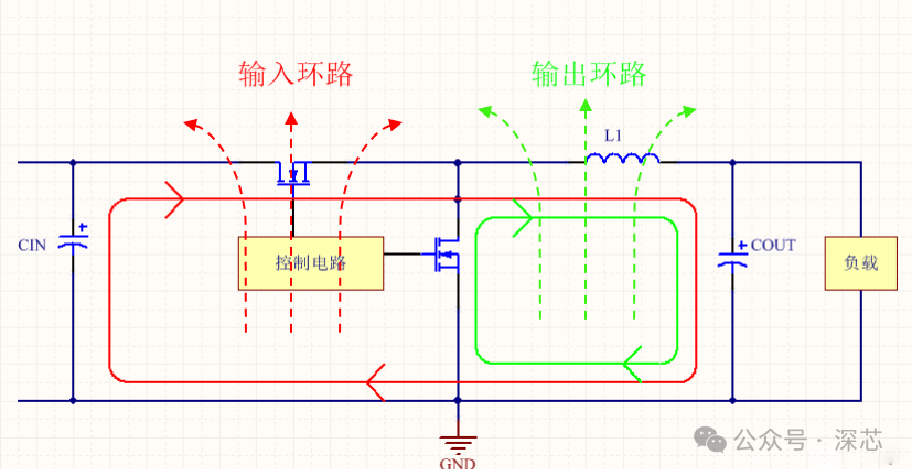
The two loops in the diagram act like antennas; the larger the loop area, the more severe the electromagnetic interference (EMI).
-
Input Loop (Vin-Cin-IC-GND): The current in this loop is discontinuous and fluctuates, exhibiting a high di/dt (current change rate), which is a major source of high-frequency noise and EMI. Therefore, minimizing the area of the input loop should be prioritized during layout.
-
Output Loop (SW-L-Cout-GND): The current in this loop is relatively continuous and smooth due to the inductance’s continuous flow effect. Although the area should also be minimized, it is of lower priority than the input loop.
Core Component Layout and Wiring
-
Input Capacitor (CIN)
The input capacitor is the first line of defense against switching noise, and its layout plays a decisive role in the area of the input loop.
-
Close to Pins: Place it as close as possible to the chip’s Vin and power ground (PGND) pins.
-
Series and Parallel: The power should first pass through the input capacitor before entering the chip pins. Large-value electrolytic or tantalum capacitors often have poor high-frequency characteristics, so a high-frequency ceramic decoupling capacitor (CBYPASS) should be placed in parallel next to it.
-
Grounding: The ground terminal of the input capacitor should be directly connected to the chip’s PGND pin, rather than through long traces to the common ground plane.
-
Power Inductor (L) and SW Node
-
Close to SW Pin: The power inductor should be placed as close as possible to the chip’s SW (switch node) pin to minimize loop area.
-
SW Node Handling: The voltage at the SW node changes rapidly at high frequencies, making it a significant noise source.
-
Short and Thick Traces: The connection from SW to the inductor should use short and thick traces or copper pours to reduce parasitic inductance and resistance.
-
Area Minimization: The copper area at the SW node should be kept as small as possible while meeting current-carrying capacity to avoid becoming an “antenna” that radiates noise.
-
Away from Sensitive Signals: Absolutely avoid routing sensitive signal lines (such as feedback lines and analog signal lines) under or near the SW node or inductor.
-
Output Capacitor (COUT)
The output capacitor is used to further filter noise and stabilize the output voltage.
Close to Inductor and GND: The output capacitor should be placed close to the power inductor and the chip’s GND pin to minimize the output loop area.
-
Feedback Network (FB)
The feedback path is the “sensor” of the chip and is easily disturbed; improper handling can lead to unstable output voltage and increased ripple.
-
Away from Noise Sources: The traces of the feedback path (especially the FB pin and voltage divider resistors) must be kept away from inductors, SW nodes, diodes, and other noise sources.
-
Short and Direct Traces: The voltage divider resistors should be placed as close as possible to the FB pin, with short traces.
-
Correct Sampling Point: The feedback voltage sampling point must be taken from the load side or the positive terminal of the output capacitor, rather than from the inductor pin, to accurately reflect the real output voltage.
-
Ground Isolation: The signal ground (AGND) of the feedback network should be separated from the power ground (PGND), typically using a “single-point connection” to avoid noise interference from the power ground affecting the sensitive reference ground. The resistance values of the feedback resistors should not be too large, with a total recommended value around 100kΩ.
-
Bootstrap Capacitor (CBST)
Close to IC: The bootstrap capacitor (if required by the chip) must be placed close to the chip’s BST and SW pins to ensure the bootstrap circuit operates correctly and quickly.
Other General Recommendations
-
Ground and Via: The power ground (PGND) should use a large area of copper pour and multiple vias connected to the internal ground plane to facilitate heat dissipation and reduce impedance. It is important to distinguish between power ground and signal ground.
-
Thermal Management: For high current applications, sufficient heat dissipation area and vias should be provided for the chip and inductor to prevent overheating.
-
Reference Manual: The ultimate guide is always the layout recommendations in the chip’s official datasheet.
Checklist
| Check Item | Description |
|---|---|
| Input capacitor close to chip Vin and PGND pins | Minimize input loop area, reduce EMI |
| Input capacitor in parallel with high-frequency decoupling capacitor | Filter out high-frequency noise, improve response speed |
| Power inductor close to chip SW pin | Reduce switch node area, lower radiation |
| SW traces short and thick, or use copper pour | Reduce parasitic inductance and voltage drop |
| SW copper area meets current but is not excessive | Prevent becoming an antenna, radiating noise |
| Output capacitor close to inductor and chip GND | Minimize output loop area, optimize output filtering |
| Feedback path away from inductors, SW, and other noise sources | Prevent noise coupling, avoid system instability |
| Feedback sampling point at output capacitor or load side | Accurate sampling of output voltage, improve voltage regulation accuracy |
| Signal ground (AGND) connected to power ground (PGND) at a single point | Prevent power ground noise from interfering with sensitive control signals |
| Bootstrap capacitor close to chip BST and SW pins | Ensure bootstrap circuit operates normally |
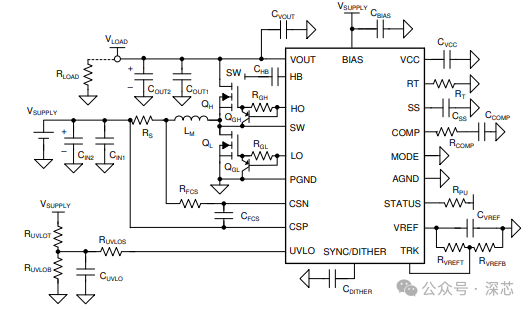
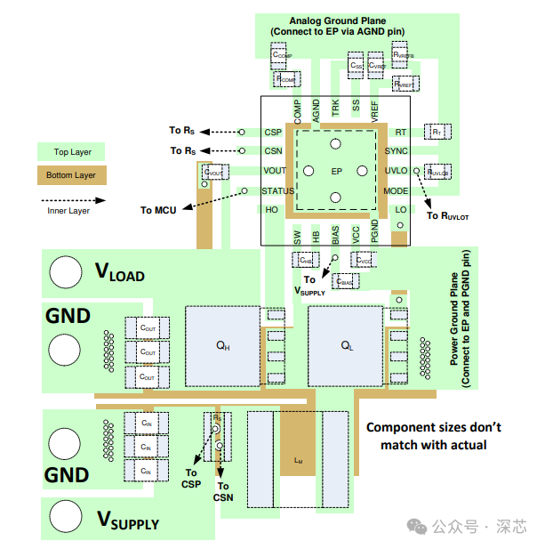
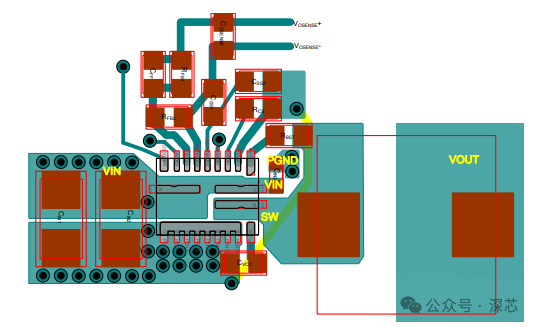
Example 1
Example 2