4. PCB Prototyping and Soldering
JLCPCB EDA not only supports one-click ordering for PCB prototyping at JLCPCB Group’s factories but also allows users to export commonly used PCB processing files such as Bill of Materials (BOM), Gerber files, coordinate files, etc., for production at any other PCB manufacturer.
1. PCB Prototyping
Click on the main menu “Order, PCB Order” to pop up a “Warning” window, prompting whether to check DRC (or other items). If confirmed that there are no issues, click “No, continue to export,” as shown in Figure 1-5-1.
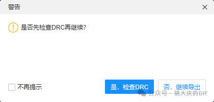
Figure 1-5-1 Continue exporting if DRC has been checked
After a moment, the “PCB Order” window will pop up, click “Confirm“, as shown in Figure 1-5-2.
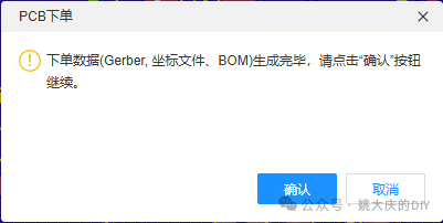
Figure 1-5-2 Confirm PCB order
Next, the basic information of the PCB will be displayed, as shown in Figure 1-5-3, where you need to select material, quantity, and other information. If you have a coupon, you can choose to use it to offset the cost. Currently, boards with a length and width not exceeding 10 cm can use the coupon. Confirm everything is correct before submitting the order.
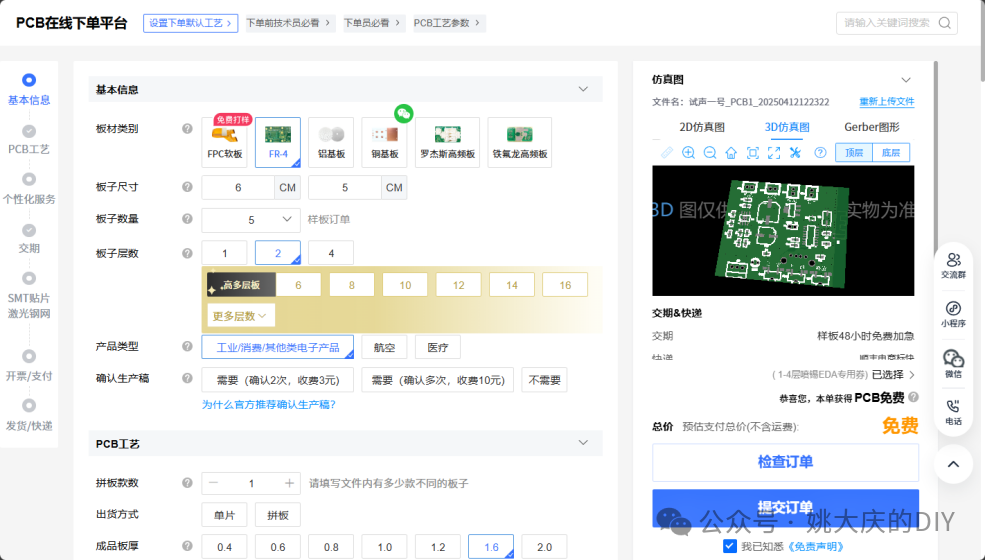
Figure 1-5-3 Set basic PCB information
In the final payment step, if a coupon is used and the amount is 0 yuan, you still need to click “Pay”; of course, the payment amount is “0 yuan,” as shown in Figure 1-5-4.
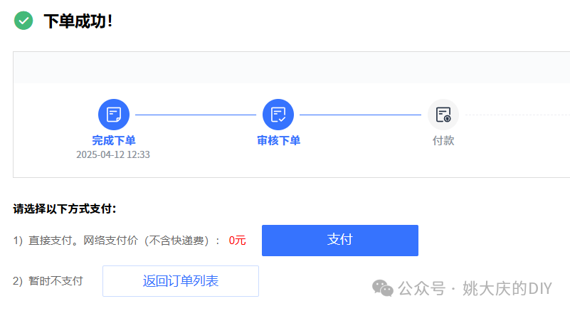
Figure 1-5-4 Payment operation is required even if the amount is 0 yuan
|
Using JLCPCB’s free coupon for prototyping is not only free but also includes free shipping. Go to the JLCPCB homepage (https://www.jlc.com/), find the “Coupon Center,” and follow the website prompts to receive it. Currently, you can receive 2 coupons per month. |
After payment is completed, you can wait for the PCB to arrive. For details about the PCB order, progress tracking, etc., you can check the ordering platform, as shown in Figure 1-5-5.
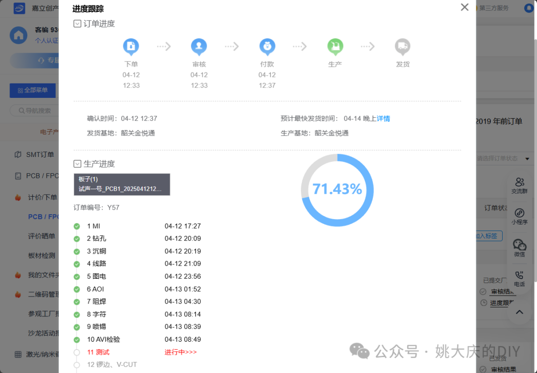
Figure 1-5-5 Check PCB order details
2. Manual Soldering of PCB
Most components in this circuit are surface-mounted, with a few through-hole components. The soldering sequence is to solder surface-mounted components first, followed by through-hole components. If the order is not appropriate, it may lead to difficulties in soldering subsequent components.
To solder surface-mounted components, you will need solder paste, flux, and a soldering station. It is recommended to use lead-containing solder with 63% tin, which has a melting point of 183 degrees and is relatively easy to solder. A no-clean, neutral flux is recommended. A digital temperature-controlled soldering station is preferred; if unavailable, a hot air gun can be used. For soldering a small number of PCBs, syringe-packaged solder paste and flux can be used, as shown in Figure 1-6-1.
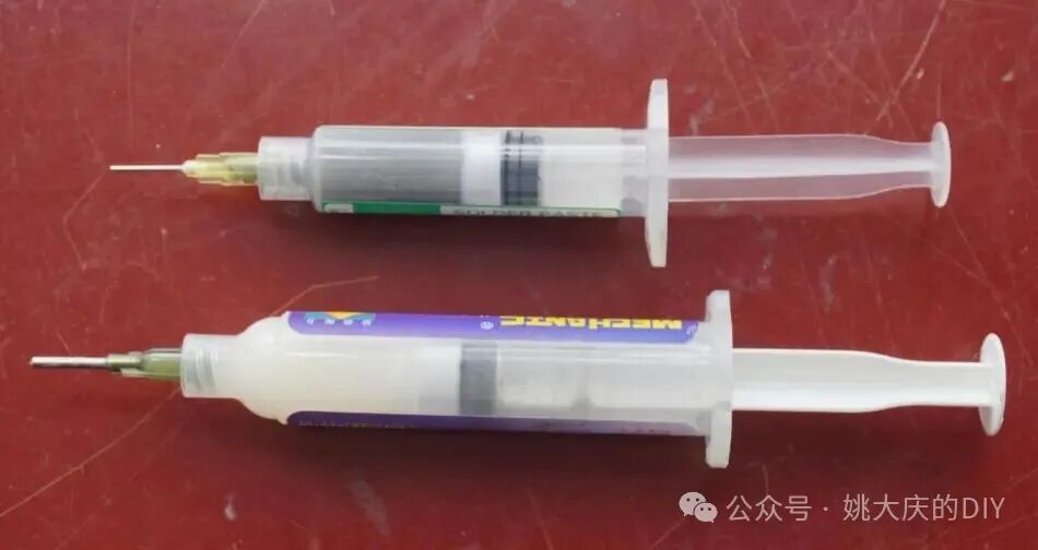
Figure 1-6-1 Syringe-packaged solder paste and flux
(1) Applying Solder Paste
Slightly press the piston of the solder paste syringe to apply solder paste onto the pads on the PCB, with the amount of solder paste forming a slight mound, as shown in Figure 1-6-2. If you are using the syringe for the first time, you may lack experience, so it is advisable to practice on larger pads first.
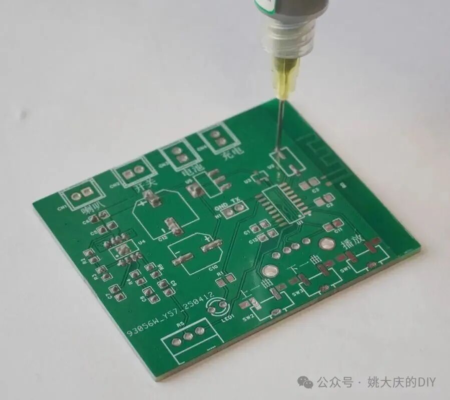
Figure 1-6-2 Applying solder paste with a syringe
Try not to spread the solder paste on a single pad; otherwise, when heated, the solder paste will not coalesce. For densely pin-packed components, be careful not to apply too much solder paste. If too much solder paste is applied and they connect, do not attempt to wipe it off, as this will make it messier; it is recommended to handle it during the subsequent soldering process.
Confirm that all pads requiring surface mounting have solder paste applied before proceeding to the next step.
(2) Placing Surface-Mounted Components
Use pointed tweezers to hold the component and align it with the pad for placement, as shown in Figure 1-6-3.
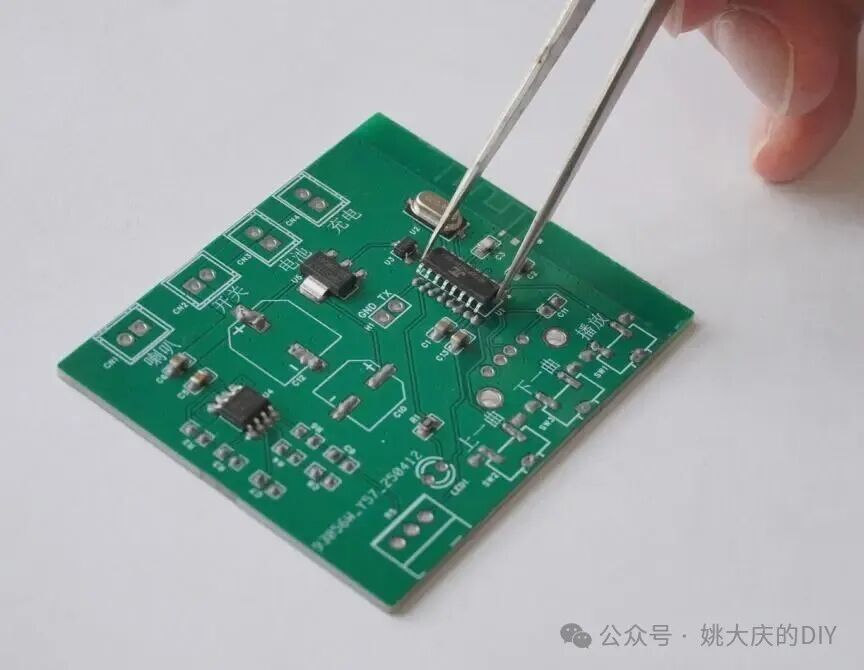
Figure 1-6-3 Placing components with pointed tweezers
Sometimes the tweezers may stick to the solder paste, making it difficult to place the component. You can clean the tweezers with alcohol or board cleaning solution, or use a second pair of tweezers for assistance. The order of placement is generally to place smaller resistors and capacitors first, then chips, and finally larger electrolytic capacitors.
(3) Soldering Surface-Mounted Components
Set the temperature of the heating station to 250 degrees (for medium-temperature 183-degree solder paste), and after stabilizing the temperature for a minute or two, carefully place the PCB with the components on the heating station. The flux in the solder paste will start to smoke, and the solder paste will begin to melt, as shown in Figure 1-6-4.
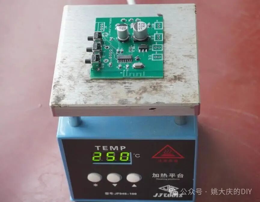
Figure 1-6-4 Soldering PCB with heating station
At this point, be aware that once the solder paste melts, it will create a significant adhesive effect, sometimes causing automatic alignment with the pads. Sometimes, the melting progress of several pads may vary, causing the component to stand upright or even flip. If this happens, promptly correct it with tweezers.
Once all the solder paste on the pads has melted, carefully hold the PCB with tweezers or pliers and slowly remove it (the solder is still in a molten state), placing it on a heat-resistant wooden board or other object to cool.
If during the solder paste application, some pads had too much solder paste, once melted, the solder may cover the surrounding pads. After the solder on the PCB has solidified, you can address this by melting the excess solder with a soldering iron and using desoldering braid or wire with a bit of flux to absorb the solder.
(4) Soldering Through-Hole Components
Through-hole components are soldered using an electric soldering iron and solder wire, with a chisel tip soldering iron recommended for fast heat transfer and ease of soldering, as shown in Figure 1-6-5. Components like potentiometers and USB sockets require precise installation positions. If all pins are soldered at once and the component is misaligned, it will be difficult to adjust. Therefore, solder one pin first, check the position and angle, and adjust if necessary before soldering the remaining pins. Larger pads dissipate heat quickly, so be decisive in feeding in a larger amount of solder to maintain rapid heat transfer from the soldering iron.
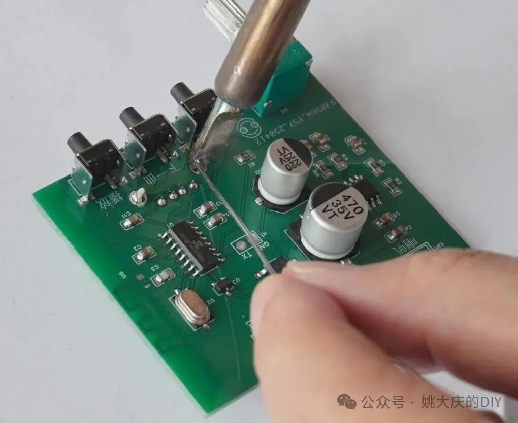
Figure 1-6-5 Recommended chisel tip soldering iron for soldering through-hole components
Figure 1-6-6 shows a comparison between the soldered PCB and the effect diagram.
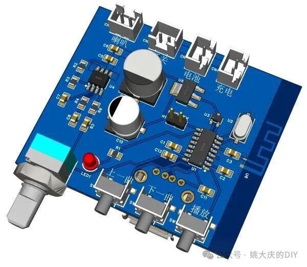
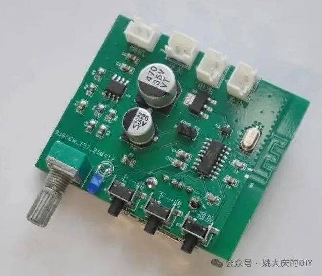
Figure 1-6-6 PCB effect diagram (left), finished product (right)
The next article will introduce the basic knowledge of entry-level development for Jieli chips, stay tuned.