 2025/02/19, Advanced Photonics News The optoelectronic integrated chip layout and tape-out service product line integrates a multi-material system, providing vertical integration from EPDA tools, PDK development, tape-out to applications. Targeting high-speed optical communication, integrated optoelectronic sensing, integrated optical computing, integrated lidar, and integrated quantum information fields, we offer tape-out, packaging, and testing services for silicon-based optoelectronic chips and III-V optoelectronic chips.
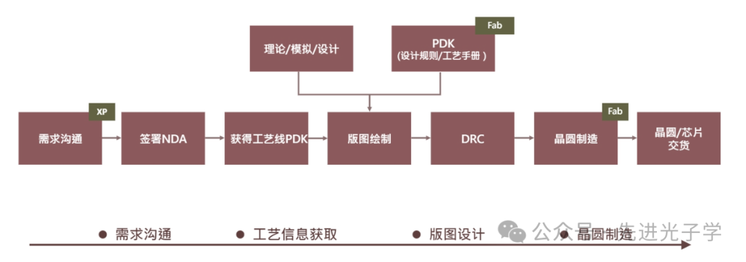 Figure 1. Full Process from Layout Design to Chip Delivery
Optoelectronic Integrated Chip Layout Services
The optoelectronic integrated chip layout and tape-out service product line has a professional optoelectronic integration support team, well-versed in the industry’s advanced optoelectronic integration design frameworks and tools, providing comprehensive EDA solutions in hotspot areas such as integrated optical frequency combs, integrated optical computing, and integrated lidar.
-
Layout Services: Professional layout drawing based on specified tape-out platform and PDK for existing designs. Layout considers Design Rule Check (DRC), Layout vs. Schematic (LVS), as well as testing and packaging design rules;
-
Layout Review: Providing manufacturing, testing, and packaging suggestions for the layout;
-
PDK Development: Customizing PDK according to specified optoelectronic integrated tape-out platforms, applicable to tape-out platforms or dedicated device libraries for end-users.
Optoelectronic Integrated Multi-Material System Chip Tape-Out Services
The optoelectronic integrated chip layout and tape-out service product line closely collaborates with multi-material system tape-out platforms to provide solutions across multiple dimensions including cost, time, performance, reliability, and yield.
The multi-material system tape-out service includes customized wafer packaging services and MPW tape-out services.
-
Silicon and Silicon Substrates: SOI, Si3N4, SiO2/PLC;
-
III-V Materials: InP;
-
Lithium Niobate: LNOI;
-
Heterogeneous Integration: SiN-on-SOI, LNOI-on-SOI, LNOI-on-SiN.
For more details on the optoelectronic integrated chip layout and tape-out services, please contact:
Sales Contact: Xiao Guang
Sales Phone: 18811555924
Email: [email protected]
He Yue Technology | X PHOTONICS
He Yue Technology (X PHOTONICS) focuses on the field of optoelectronic integration technology. It provides Chinese users with optoelectronic integrated layout implementation services, optoelectronic hybrid packaging testing equipment and services, ultrafast laser processing equipment and services, as well as multi-material system semiconductor (SOI/Si3N4/LNOI/SiO2) tape-out services. Technical collaborations involve silicon photonic communication optical modules, integrated lidar modules, integrated optical frequency comb chips, integrated optical quantum information chips, super-resolution imaging optoelectronic chips, and biomedical optoelectronic chips.

Advanced Photonics
“Advanced Photonics” is a media outlet in the optoelectronic field, focusing on the stage of technology research transformation into mass-produced products. It introduces technologies and products with batch application prospects, publishes market analysis reports, compiles information on industry exhibitions, industrial forums, and technical exchange meetings, and selects books and materials related to market hotspots.
Advanced Photonics WeChat Subscription Account

Advanced Photonics WeChat Personal Account
Xiao Guang 18811555924 (WeChat same number)
Copyright Statement
This article’s copyright belongs to the original author and the material provider. If the content involves copyright and other issues, please contact the above phone number or WeChat immediately.