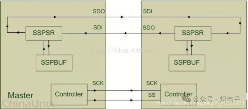
The SPI interface (Serial Peripheral Interface) is a synchronous serial communication protocol widely used for high-speed data exchange between devices over short distances. Its core features and technical details are as follows:
Communication Modes
- Uses a master-slave architecture, supporting communication between a single master and one or more slave devices, with the master device managing the slave devices through a chip select signal (CS/SS).
- Full-duplex synchronous communication, with data transfer rates exceeding 100 MHz.
- Hardware Structure
- SCLK: The synchronous clock signal provided by the master device;
- MOSI: Master output, slave input data line;
- MISO: Master input, slave output data line;
- CS/SS: Slave chip select signal line.
 Four modes of the SPI bus: CPOL and CPHA.CPOL indicates the level state of the SPI bus clock when idle, where 0 represents low level and 1 represents high level.CPHA indicates which clock edge is sampled, where 0 indicates the first clock edge and 1 indicates the second clock edge.
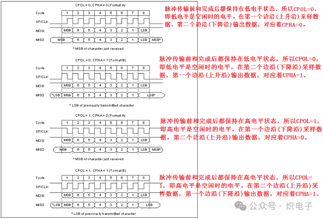 Objective of this experiment: Based on the Black Gold platform, implement SPI Master code for FPGA access to M25P16 SPI Flash, including reading the content of the first byte at address 000000, as well as reading the manufacturer ID and device ID of the M25P16.Project Structure:
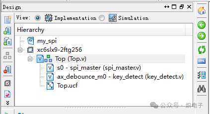 Hardware Structure:
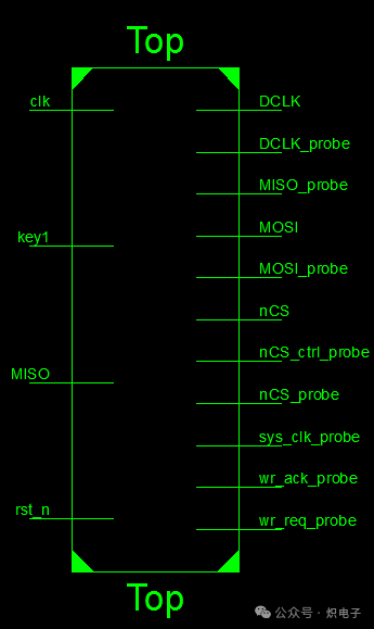 top.v
top.v
`timescale 1ns / 1ps
// Create a state machine to input commands to spi_master in sequence
module Top(    input       clk,    input       rst_n,    output      nCS,            output      DCLK,                output      MOSI,                input       MISO,    input       key1,                    // Button triggers transition from IDLE to SEND state
    output      MISO_probe,    output      nCS_ctrl_probe,    output      sys_clk_probe,        output      wr_req_probe,        output      DCLK_probe,        output      MOSI_probe,            output      nCS_probe,            output      wr_ack_probe    );

/* State machine encoding */localparam  S_IDLE = 4'd0;localparam  S_SEND = 4'd1;localparam  S_RECV = 4'd2;
/* Fixed data */localparam  DATA0 = 8'h03;localparam  DATA1 = 8'h00;localparam  DATA2 = 8'h00;localparam  DATA3 = 8'h00;

reg [7:0]  data_in;        wire [7:0]  data_out;//reg     wr_req;wire     wr_ack;
reg     nCS_ctrl;
reg [3:0] state;reg [3:0] next_state;
reg [7:0] send_cnt;reg [7:0] recv_cnt;
reg     wr_ack_d0;reg     wr_ack_d1;wire     wr_ack_pos;        // Detect rising edge
assign wr_ack_pos = wr_ack_d0 & ~wr_ack_d1;
wire      button_negedge;
/*  */


always @(posedge clk or negedge rst_n) begin    if(rst_n == 1'b0)begin        wr_ack_d0 <= 1'b0;        wr_ack_d1 <= 1'b0;end
elsebegin        wr_ack_d0 <= wr_ack;        wr_ack_d1 <= wr_ack_d0;end
end


always @(posedge clk or negedge rst_n) begin    if(rst_n == 1'b0)    begin        state <= S_IDLE;    end
    else    begin        state <= next_state;        endend

/* Combinational logic */always @(*) begin    case (state)    S_IDLE:    begin        if(button_negedge == 1'b1)            next_state = S_SEND;else            next_state = S_IDLE;end
    S_SEND:begin        if(send_cnt == 8'd4)            // send_cnt finished sending count        begin            next_state = S_RECV;        end        else        begin            next_state = S_SEND;        end    end
    S_RECV:    begin        if(recv_cnt == 8'd1)            // recv_cnt finished receiving countbegin            next_state = S_IDLE;endelsebegin            next_state = S_RECV;endend
default:        next_state = S_IDLE;    endcase
end

/* Handle send_cnt */always @(posedge clk or negedge rst_n) begin    if(rst_n == 1'b0)    begin        send_cnt <= 8'd0;end
    else if(state == S_SEND)begin        if(wr_ack == 1'b1)        begin            send_cnt <= send_cnt + 8'd1;endend
    elsebegin        send_cnt <= 8'd0;    end
end

/* Handle recv_cnt */always @(posedge clk or negedge rst_n) begin    if(rst_n == 1'b0)begin        recv_cnt <= 8'd0;    end
    else if(state == S_RECV)    begin        if(wr_ack_pos == 1'b1)begin            recv_cnt <= recv_cnt + 8'd1;        end    end
    else    begin        recv_cnt <= 8'd0;end
end

/* Handle nCS_ctrl */always @(posedge clk or negedge rst_n) begin    if(rst_n == 1'b0)    begin        nCS_ctrl <= 1'd1;end
    else if(state == S_RECV || state == S_SEND)begin        nCS_ctrl <= 1'd0;    end
    else    begin        nCS_ctrl <= 1'd1;end
end

/* Handle data_in */always @(posedge clk or negedge rst_n) begin    if(rst_n == 1'b0)    begin        data_in <= 8'd0;end
    else if(state == S_SEND)begin        if(send_cnt == 8'd0)            data_in <= DATA0;        else if(send_cnt == 8'd1)            data_in <= DATA1;else if(send_cnt == 8'd2)            data_in <= DATA2;        else if(send_cnt == 8'd3)            data_in <= DATA3;endend

spi_master s0(    .sys_clk        (clk        ),        .rst            (~rst_n        ),        .nCS            (nCS        ),        .DCLK            (DCLK        ),        .MOSI            (MOSI        ),        .MISO            (MISO        ),        .CPOL            (1'b1        ),    .CPHA            (1'b1        ),    .nCS_ctrl        (nCS_ctrl        ),    .clk_div        (16'd0        ),    .wr_req            (~nCS_ctrl        ),    .wr_ack            (wr_ack        ),    .data_in        (data_in        ),    .data_out        (data_out        ),
    /* Output for logic analysis */    .MISO_probe        (MISO_probe        ),    .nCS_ctrl_probe    (nCS_ctrl_probe        ),    .sys_clk_probe    (sys_clk_probe        ),    .wr_req_probe    (wr_req_probe        ),    .DCLK_probe        (DCLK_probe        ),    .MOSI_probe        (MOSI_probe        ),    .nCS_probe        (nCS_probe        ),    .wr_ack_probe    (wr_ack_probe        )
);

/* Button detection */key_detect ax_debounce_m0(    .clk             (clk),    .rst             (~rst_n),    .button_in       (key1),    .button_posedge  (),    .button_negedge  (button_negedge),    .button_out      ());
endmodule
spi_master.v
module spi_master(    input                       sys_clk,        input                       rst,    output                      nCS,       //chip select (SPI mode)     output                      DCLK,      //spi  clock    output                      MOSI,      //spi  master data output    input                       MISO,      //spi  master input    input                       CPOL,    input                       CPHA,    input                       nCS_ctrl,    input[15:0]                 clk_div,    input                       wr_req,    output                      wr_ack,    input[7:0]                  data_in,    output[7:0]                 data_out,

/* Output for logic analysis */    output                          MISO_probe        ,    output                          nCS_ctrl_probe    ,    output                          sys_clk_probe    ,    output                          wr_req_probe    ,    output                          DCLK_probe        ,    output                          MOSI_probe        ,    output                          nCS_probe        ,    output                          wr_ack_probe
);

/* Output test signals */assign MISO_probe        = MISO;assign nCS_ctrl_probe    = nCS_ctrl;assign sys_clk_probe    = sys_clk;assign wr_req_probe    = wr_req;assign DCLK_probe        = DCLK;assign MOSI_probe        = MOSI;assign nCS_probe        = nCS;assign wr_ack_probe    = wr_ack;

localparam            IDLE            = 0;localparam            DCLK_EDGE       = 1;localparam            DCLK_IDLE       = 2;localparam            ACK             = 3;localparam            LAST_HALF_CYCLE = 4;localparam            ACK_WAIT        = 5;reg                DCLK_reg;reg[7:0]            MOSI_shift;reg[7:0]            MISO_shift;reg[2:0]            state;reg[2:0]            next_state;reg[15:0]            clk_cnt;reg[4:0]            clk_edge_cnt;

assign MOSI = MOSI_shift[7];assign DCLK = DCLK_reg;assign data_out = MISO_shift;assign wr_ack = (state == ACK);assign nCS = nCS_ctrl;

always@(posedge sys_clk or posedge rst)beginif(rst)        state <= IDLE;else        state <= next_state;end

always@(*)begincase(state)        IDLE:            if(wr_req == 1'b1)                next_state <= DCLK_IDLE;else                next_state <= IDLE;        DCLK_IDLE://half a SPI clock cycle produces a clock edgeif(clk_cnt == clk_div)                next_state <= DCLK_EDGE;else                next_state <= DCLK_IDLE;        DCLK_EDGE://a SPI byte with a total of 16 clock edgesif(clk_edge_cnt == 5'd15)                next_state <= LAST_HALF_CYCLE;else                next_state <= DCLK_IDLE;//this is the last data edge                LAST_HALF_CYCLE:if(clk_cnt == clk_div)                next_state <= ACK;else                next_state <= LAST_HALF_CYCLE; //send one byte complete                ACK:            next_state <= ACK_WAIT;//wait for one clock cycle, to ensure that the cancel request signal        ACK_WAIT:            next_state <= IDLE;default:            next_state <= IDLE;    endcaseend

always@(posedge sys_clk or posedge rst)beginif(rst)        DCLK_reg <= 1'b0;else if(state == IDLE)        DCLK_reg <= CPOL;else if(state == DCLK_EDGE)        DCLK_reg <= ~DCLK_reg;//SPI clock edgeend

//SPI clock wait counteralways@(posedge sys_clk or posedge rst)beginif(rst)        clk_cnt <= 16'd0;else if(state == DCLK_IDLE || state == LAST_HALF_CYCLE)         clk_cnt <= clk_cnt + 16'd1;else        clk_cnt <= 16'd0;end
//SPI clock edge counteralways@(posedge sys_clk or posedge rst)beginif(rst)        clk_edge_cnt <= 5'd0;else if(state == DCLK_EDGE)        clk_edge_cnt <= clk_edge_cnt + 5'd1;else if(state == IDLE)        clk_edge_cnt <= 5'd0;end
//SPI data outputalways@(posedge sys_clk or posedge rst)beginif(rst)        MOSI_shift <= 8'd0;else if(state == IDLE && wr_req)        MOSI_shift <= data_in;else if(state == DCLK_EDGE)if(CPHA == 1'b0 && clk_edge_cnt[0] == 1'b1)            MOSI_shift <= {MOSI_shift[6:0],MOSI_shift[7]};else if(CPHA == 1'b1 && (clk_edge_cnt != 5'd0 && clk_edge_cnt[0] == 1'b0))            MOSI_shift <= {MOSI_shift[6:0],MOSI_shift[7]};end
//SPI data inputalways@(posedge sys_clk or posedge rst)beginif(rst)        MISO_shift <= 8'd0;else if(state == IDLE && wr_req)        MISO_shift <= 8'h00;else if(state == DCLK_EDGE)if(CPHA == 1'b0 && clk_edge_cnt[0] == 1'b0)            MISO_shift <= {MISO_shift[6:0],MISO};else if(CPHA == 1'b1 && (clk_edge_cnt[0] == 1'b1))            MISO_shift <= {MISO_shift[6:0],MISO};end

endmodule
key_detect.v
`timescale 1 ns / 100 ps
module  key_detect (    input       clk,     input       rst,     input       button_in,    output reg  button_posedge,    output reg  button_negedge,    output reg  button_out);
//// ---------------- internal constants --------------
parameter N = 32 ;           // debounce timer bitwidth
parameter FREQ = 50;         //model clock :Mhz
parameter MAX_TIME = 20;     //ms
localparam TIMER_MAX_VAL =   MAX_TIME * 1000 * FREQ;
////---------------- internal variables ---------------
reg  [N-1 : 0]  q_reg;      // timing regs
reg  [N-1 : 0]  q_next;
reg DFF1, DFF2;             // input flip-flops
wire q_add;                 // control flags
wire q_reset;
reg button_out_d0;
//// ------------------------------------------------------
//// Continuous assignment for counter control
assign q_reset = (DFF1  ^ DFF2);          // xor input flip flops to look for level change to reset counter
assign q_add = ~(q_reg == TIMER_MAX_VAL); // add to counter when q_reg msb is equal to 0
//// Combo counter to manage q_next always @ ( q_reset, q_add, q_reg)begin    case( {q_reset , q_add})        2'b00 :                q_next <= q_reg;        2'b01 :                q_next <= q_reg + 1;        default :                q_next <= { N {1'b0} };    endcase     end
//// Flip flop inputs and q_reg update
always @ ( posedge clk or posedge rst)begin    if(rst == 1'b1)    begin        DFF1 <= 1'b0;        DFF2 <= 1'b0;        q_reg <= { N {1'b0} };    end    else    begin        DFF1 <= button_in;        DFF2 <= DFF1;        q_reg <= q_next;    endend
//// Counter control
always @ ( posedge clk or posedge rst)beginif(rst == 1'b1)        button_out <= 1'b1;    else if(q_reg == TIMER_MAX_VAL)        button_out <= DFF2;    else        button_out <= button_out;end
always @ ( posedge clk or posedge rst)beginif(rst == 1'b1)    begin        button_out_d0 <= 1'b1;        button_posedge <= 1'b0;        button_negedge <= 1'b0;    endelse    begin        button_out_d0 <= button_out;        button_posedge <= ~button_out_d0 & button_out;        button_negedge <= button_out_d0 & ~button_out;    end    endendmodule
Pin Constraint File Top.ucf
NET "clk" IOSTANDARD = LVCMOS33;
NET "DCLK" IOSTANDARD = LVCMOS33;
NET "DCLK_probe" IOSTANDARD = LVCMOS33;
NET "MISO" IOSTANDARD = LVCMOS33;
NET "MISO_probe" IOSTANDARD = LVCMOS33;
NET "MOSI" IOSTANDARD = LVCMOS33;
NET "MOSI_probe" IOSTANDARD = LVCMOS33;
NET "nCS" IOSTANDARD = LVCMOS33;
NET "nCS_ctrl_probe" IOSTANDARD = LVCMOS33;
NET "nCS_probe" IOSTANDARD = LVCMOS33;
NET "sys_clk_probe" IOSTANDARD = LVCMOS33;
NET "wr_ack_probe" IOSTANDARD = LVCMOS33;
NET "wr_req_probe" IOSTANDARD = LVCMOS33;
NET "rst_n" IOSTANDARD = LVCMOS33;

NET "clk" LOC = T8;
NET "DCLK" LOC = R11;
NET "DCLK_probe" LOC = M4;
NET "MISO" LOC = P10;
NET "MISO_probe" LOC = N4;
NET "MOSI" LOC = T10;
NET "MOSI_probe" LOC = P2;
NET "nCS" LOC = T3;
NET "nCS_ctrl_probe" LOC = M5;
NET "nCS_probe" LOC = R2;
NET "rst_n" LOC = L3;
NET "sys_clk_probe" LOC = N6;
NET "wr_ack_probe" LOC = R1;
NET "wr_req_probe" LOC = P6;
# PlanAhead Generated physical constraints
NET "key1" LOC = C3;
# PlanAhead Generated IO constraints
NET "key1" IOSTANDARD = LVCMOS33;
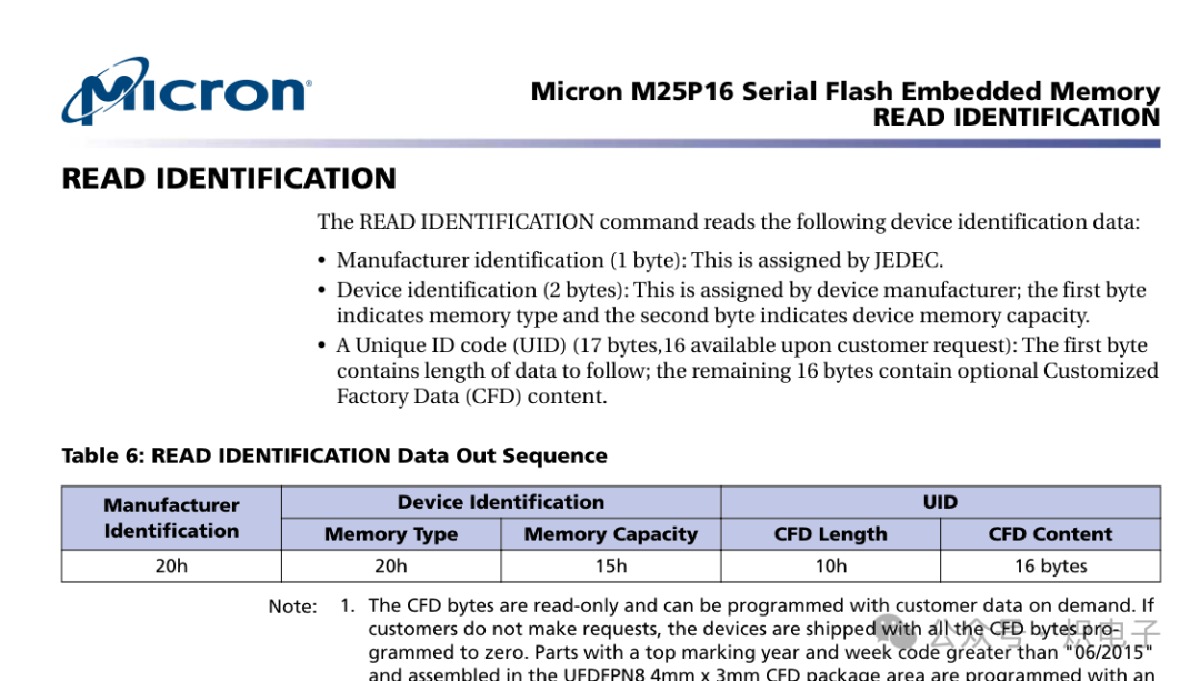
Experiment Phenomenon 1: After compiling and programming the FPGA firmware, pressing the key1 button on the development board captured the SPI communication waveform with a logic analyzer, where the FPGA first sent the 03h command and the 000000 address, then read 1 byte of data 0E (the data written by the official Black Gold example).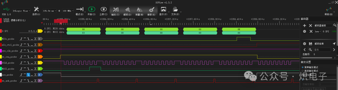 The preceding code implements data reading, and below is the code for reading the manufacturer ID and device ID of the M25P16, which only requires modifying the data in top.v, as shown in the modified code below.Top.v
`timescale 1ns / 1ps
// Create a state machine to input commands to spi_master in sequence
module my_spi_top_2(    input       clk,    input       rst_n,    output      nCS,            output      DCLK,                output      MOSI,                input       MISO,    input           key1,                    // Button triggers transition from IDLE to SEND state
/* Connect signals for logic analysis */    output      MISO_probe,    output      nCS_ctrl_probe,    output      sys_clk_probe,        output      wr_req_probe,        output      DCLK_probe,        output      MOSI_probe,            output      nCS_probe,            output      wr_ack_probe    );

/* State machine encoding */localparam  S_IDLE = 4'd0;localparam  S_SEND = 4'd1;localparam  S_RECV = 4'd2;
/* Fixed data, "READ IDENTIFICATION", the ID command for the M25P16 storage chip is 9Fh, 9Eh */localparam  DATA0 = 8'h9f;localparam  DATA1 = 8'h9e;localparam  DATA2 = 8'h00;localparam  DATA3 = 8'h00;

reg [7:0]  data_in;        wire [7:0]  data_out;//reg     wr_req;wire     wr_ack;
reg     nCS_ctrl;
reg [3:0] state;reg [3:0] next_state;
reg [7:0] send_cnt;reg [7:0] recv_cnt;
reg     wr_ack_d0;reg     wr_ack_d1;wire     wr_ack_pos;        // Detect rising edge
assign wr_ack_pos = wr_ack_d0 & ~wr_ack_d1;
wire      button_negedge;
/*  */


always @(posedge clk or negedge rst_n) begin    if(rst_n == 1'b0)begin        wr_ack_d0 <= 1'b0;        wr_ack_d1 <= 1'b0;end
elsebegin        wr_ack_d0 <= wr_ack;        wr_ack_d1 <= wr_ack_d0;end
end


always @(posedge clk or negedge rst_n) begin    if(rst_n == 1'b0)    begin        state <= S_IDLE;    end
    else    begin        state <= next_state;        endend

/* Combinational logic */always @(*) begin    case (state)    S_IDLE:    begin        if(button_negedge == 1'b1)            next_state = S_SEND;else            next_state = S_IDLE;end
    S_SEND:begin        if(send_cnt == 8'd2)            // send_cnt finished sending count, 9fh, 9eh commands require sending 2 bytes of data        begin            next_state = S_RECV;        end        else        begin            next_state = S_SEND;        end    end
    S_RECV:    begin        if(recv_cnt == 8'd20)            // recv_cnt finished receiving count, 9eh command reads back 20 bytes of data, including Manufacturer ID (EFh) and Device IDbegin            next_state = S_IDLE;endelsebegin            next_state = S_RECV;endend
default:        next_state = S_IDLE;    endcase
end

/* Handle send_cnt */always @(posedge clk or negedge rst_n) begin    if(rst_n == 1'b0)    begin        send_cnt <= 8'd0;end
    else if(state == S_SEND)begin        if(wr_ack == 1'b1)        begin            send_cnt <= send_cnt + 8'd1;endend
    elsebegin        send_cnt <= 8'd0;    end
end

/* Handle recv_cnt */always @(posedge clk or negedge rst_n) begin    if(rst_n == 1'b0)begin        recv_cnt <= 8'd0;    end
    else if(state == S_RECV)    begin        if(wr_ack_pos == 1'b1)begin            recv_cnt <= recv_cnt + 8'd1;        end    end
    else    begin        recv_cnt <= 8'd0;end
end

/* Handle nCS_ctrl */always @(posedge clk or negedge rst_n) begin    if(rst_n == 1'b0)    begin        nCS_ctrl <= 1'd1;end
    else if(state == S_RECV || state == S_SEND)begin        nCS_ctrl <= 1'd0;    end
    else    begin        nCS_ctrl <= 1'd1;end
end

/* Handle data_in */always @(posedge clk or negedge rst_n) begin    if(rst_n == 1'b0)    begin        data_in <= 8'd0;end
    else if(state == S_SEND)begin        if(send_cnt == 8'd0)            data_in <= DATA0;        else if(send_cnt == 8'd1)            data_in <= DATA1;else if(send_cnt == 8'd2)            data_in <= DATA2;        else if(send_cnt == 8'd3)            data_in <= DATA3;endend

spi_master s0(    .sys_clk        (clk        ),        .rst            (~rst_n        ),        .nCS            (nCS        ),        .DCLK            (DCLK        ),        .MOSI            (MOSI        ),        .MISO            (MISO        ),        .CPOL            (1'b1        ),    .CPHA            (1'b1        ),    .nCS_ctrl        (nCS_ctrl        ),    .clk_div        (16'd0        ),    .wr_req            (~nCS_ctrl        ),    .wr_ack            (wr_ack        ),    .data_in        (data_in        ),    .data_out        (data_out        ),
    /* Output for logic analysis */    .MISO_probe        (MISO_probe        ),    .nCS_ctrl_probe    (nCS_ctrl_probe        ),    .sys_clk_probe    (sys_clk_probe        ),    .wr_req_probe    (wr_req_probe        ),    .DCLK_probe        (DCLK_probe        ),    .MOSI_probe        (MOSI_probe        ),    .nCS_probe        (nCS_probe        ),    .wr_ack_probe    (wr_ack_probe        )
);

/* Button detection */key_detect ax_debounce_m0(    .clk             (clk),    .rst             (~rst_n),    .button_in       (key1),    .button_posedge  (),    .button_negedge  (button_negedge),    .button_out      ());
endmodule
Experiment Phenomenon 2: After compiling and programming the FPGA firmware, pressing key1, the FPGA sent the commands specified in the M25P16 datasheet, 9fh and 9eh, and read the corresponding IDs.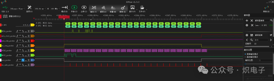 M25P16 Datasheet: