Introduction
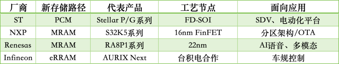
In 2025, within just six months, leading MCU manufacturers such as ST, NXP, and Renesas simultaneously released automotive MCU products equipped with new types of embedded storage (such as PCM and MRAM), breaking the long-standing technical pattern dominated by embedded Flash. While it is still too early to talk about a “standard configuration,” it is certain that new storage has transitioned from “experimentation” to “strategic layout” and is beginning to have a profound impact on the MCU ecosystem.
In the past, MCUs were considered “small and beautiful” devices used for basic control logic. However, in recent years, they have been evolving towards “small and powerful”: processes have advanced from traditional 40nm to 22nm, 16nm, and even more advanced nodes; integrating AI acceleration, security units, wireless modules… has made them candidates for the “brain of the car” and “central hub of edge computing”.
Behind this evolution, a long-overlooked but crucial technology is “filling the gaps”: the revolution of embedded storage technology (eNVM).
Under the trend of “software-defined vehicles,” OEMs and Tier 1 manufacturers face unprecedented challenges: the complexity of ECUs is skyrocketing, and functions are highly centralized; OTA updates, AI inference, and model loading are making software “thicker and thicker”; storage space and read/write performance have become bottlenecks in the vehicle architecture. Traditional Flash has long been inadequate in terms of density, speed, power consumption, and durability. In this context, new types of memory (PCM, MRAM) have become key weapons for MCU evolution.
Scan the code to reply“MCU” keywords to join the industry group and receive the report
ST Chooses Phase Change Memory (PCM)
Phase Change Memory (PCM) is an emerging non-volatile storage technology based on the principle of storing information through the phase change of materials (from amorphous to crystalline). The basic mechanism of PCM was invented by Robert Ovshinsky at Stanford University in the 1960s. STMicroelectronics holds the patent for this original development, making it the first company to implement PCM in automotive-grade MCUs.
ST also introduced the working principle of PCM on its official website, stating that PCM is made from a germanium-antimony-telluride (GST) alloy, which utilizes the physical property of materials to undergo rapid thermal control changes between amorphous and crystalline states during manufacturing. These states correspond to logical 0 and logical 1, which can be electrically distinguished by the high resistance of the amorphous state (logical 0) and the low resistance of the crystalline state (logical 1). PCM supports read/write operations at low voltage and has several substantial advantages over Flash and other embedded storage technologies.
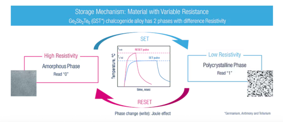
Working principle of PCM (Image source: ST)
After years of research and development, in April 2025, ST launched the Stellar with xMemory, which is a new generation of scalable memory embedded in its Stellar series of automotive microcontrollers. The core of Stellar xMemory is STMicroelectronics’ proprietary phase change memory (PCM) technology. ST claims to have the industry’s smallest qualified storage bit unit, which can fundamentally change the challenging process of developing software-defined vehicles (SDVs) and evolving electrification platforms.
It is reported that ST’s Stellar P and G series automotive MCUs will both feature the latest generation of PCM technology with xMemory. The Stellar P and Stellar G series are suitable for centralized area controllers, domain controllers, and body applications of the Stellar Integration MCU. The first to be launched will be the Stellar P6 MCU, designed to meet the needs of the new powertrain trends and architectures for electric vehicles (EVs), which will go into production in the second half of 2025.
The Stellar with xMemory technology eliminates the need to manage multiple devices with different memory options, avoiding related development and certification costs. It provides customers with an efficient and economical solution with just one innovative device featuring scalable memory. This simplified approach from the outset allows automotive manufacturers to design for the future and leaves more room for innovation in the later stages of the development cycle, thereby reducing development costs and accelerating time-to-market through a more streamlined supply chain.
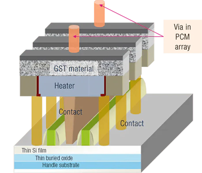
Cross-section of embedded PCM bit unit using FD-SOI technology, showing the heating device that can rapidly flip the storage unit between crystalline and amorphous states.
ST points out that choosing the right MCU at the early stage of the SDV lifecycle ensures sufficient on-chip memory for future software development. Today, selecting excessively high memory specifications increases costs, while choosing excessively low memory specifications may require subsequent searches for and re-certification of other MCUs with additional memory, thereby increasing complexity, costs, and delays. The Stellar MCU with xMemory is competitively priced, offering more cost savings, simplifying the OEM supply chain, and shortening certification time by extending product lifecycles and maximizing reuse between projects, thus accelerating time-to-market.
NXP and Renesas Embrace MRAM
Magnetoresistive RAM (MRAM) is another type of non-volatile storage “black technology” that utilizes the physical properties of magnetic materials to achieve data storage, featuring ultra-high write speeds, low power consumption, and exceptional durability. MRAM has been widely adopted by companies such as NXP and Renesas.
NXP was one of the first automotive MCU manufacturers to launch MRAM MCUs. In March of this year, NXP Semiconductors announced the launch of its S32K5 series automotive MCU, which is the industry’s first MCU based on 16nm FinFET technology with built-in MRAM, marking an important milestone in its development. The S32K5 series aims to expand NXP’s CoreRide platform, providing pre-integrated regional and electrification system solutions to support the evolution of scalable software-defined vehicle (SDV) architectures.
Automakers are increasingly adopting partitioned architectures, each with its unique approach to integrating and distributing the functions of electronic control units (ECUs). At the core of these solutions is advanced MCU architecture that combines real-time performance with low latency, deterministic communication, and innovative isolation features.
The addition of high-performance MRAM significantly accelerates ECU programming speed, whether in factory settings or during wireless (OTA) updates. The write speed of MRAM is more than 15 times faster than traditional embedded Flash, enhancing the flexibility of automakers to deploy new software features throughout the vehicle’s lifecycle.
In July 2025, Renesas also released an MCU with built-in MRAM, but with a 22nm process compared to NXP. This device is equipped with 1MB MRAM and 2MB SRAM. It is said that the use of MRAM is a major feature of the second-generation RA8 series. In addition to high durability and data retention capabilities, MRAM also offers high-speed read/write, no need for erasure, and low power consumption advantages. Renesas Electronics presented high-speed read/write technology for MRAM aimed at high-performance microcontrollers at the International Solid-State Circuits Conference (ISSCC 2024), with the RA8P1 adopting this technology.
For applications requiring larger memory capacity, this device is equipped with an eight-channel SPI interface supporting XIP/DOTF and a 32-bit external bus interface. Additionally, it offers system-in-package (SiP) products with integrated 4MB or 8MB external Flash memory. In terms of peripheral functions, it supports parallel camera input, MIPI-CSI2, serial audio input, and multi-modal AI voice input via PDM. It also features a 16-bit AD converter, graphical HMI capabilities, and various serial interfaces.
Taiwan Semiconductor Manufacturing Company: Advancing MRAM and RRAM Simultaneously
As the world’s leading foundry, TSMC is betting on two new storage technologies: MRAM and RRAM.
At the 2025 Technology Symposium, TSMC’s Executive Vice President and Co-CEO, Dr. Mark Liu, stated: “eFlash technology has encountered expansion bottlenecks at the 28nm process node, and the next generation of NVM (non-volatile memory) must replace its role in more advanced processes.”
As a result, TSMC has clearly proposed to introduce RRAM and MRAM embedded storage technologies into 22nm, 16nm, and 12nm, and further advance to 6nm and 5nm nodes.
TSMC is currently one of the few manufacturers that have achieved large-scale production of RRAM. It has already achieved RRAM mass production at 40nm, 28nm, and 22nm processes and has passed automotive-grade certification. The 12nm RRAM has also entered the customer tape-out stage, and the 6nm version is in progress. Infineon’s next-generation AURIX MCU adopts TSMC’s eRRAM technology, becoming an important embedded storage solution for its automotive platform.
The advantages of RRAM include: low process complexity, direct deployment in the back-end metal layer (BEOL); complete compatibility with logic processes, adaptable to various MCU architectures; especially suitable for power-sensitive and cost-controlled consumer and automotive applications.
In contrast, while MRAM has a more complex process, it offers superior performance characteristics: write speeds are dozens of times faster than Flash; non-volatile storage with exceptional durability; suitable for complex tasks requiring high-speed writing, frequent OTA updates, and AI inference. For in-vehicle computing platforms (such as ADAS, AI SoCs) that pursue computational density, data throughput, and real-time performance, MRAM may be the most ideal storage replacement after eFlash.
TSMC has already achieved MRAM mass production at the 22nm process node, with 16nm MRAM entering the customer preparation stage, and 12nm under development. A more aggressive roadmap also includes future expansion to the 5nm node.
In May 2025, TSMC announced the establishment of its first European Design Center (EUDC) in Munich, focusing on the research and development and customer support of MRAM storage technology for automotive applications. This center will become TSMC’s tenth design center globally and is scheduled to officially open in the third quarter of 2025, covering automotive, industrial, AI, telecommunications, and IoT fields. This also means that TSMC is not only promoting the popularization of new storage technologies on the process platform but is also deeply integrating into the vehicle development ecosystem globally.
In addition to horizontally advancing process nodes, TSMC is also seeking technological breakthroughs in the following areas:
-
3D RRAM MCU: Promoting embedded storage stacked packaging to free up more on-chip space;
-
SOT MRAM (Spin-Orbit Torque): Lower power consumption and faster writing compared to traditional STT-MRAM, expected to enter large-scale production;
-
Silicon photonic platform: Combining optical interconnects with storage interfaces, targeting data centers and edge computing layouts.
The implementation of these technologies will further consolidate TSMC’s leading position in specialty processes and the embedded storage ecosystem.
Trend of Storage-Computing Integration
Whether it is PCM, MRAM, or RRAM, they are not just substitutes for memory but catalysts for the transformation of MCU architecture. New storage technologies like PCM, MRAM, and RRAM represent a deeper trend of “storage-computing integration,” which is not merely a matter of replacing storage media but a synergistic evolution between storage architecture and computing architecture.
In the MCU field, the boundaries between storage and computing are becoming increasingly blurred. In traditional MCUs, storage and computing are separate modules, with computation performed by a central processing unit (CPU) or dedicated accelerators, while storage is managed through external or internal devices like Flash and SRAM. However, as computational tasks become more complex, especially with the growing demand for machine learning, AI inference, and edge computing applications, the separation of storage and computing is becoming increasingly inadequate.
The introduction of new storage devices like MRAM and PCM provides a new opportunity for “storage-computing integration.” Particularly, PCM, through its phase change characteristics, not only possesses non-volatile storage capabilities but can also play a role in “near-computation” in certain applications, reducing data transfer bottlenecks and further accelerating data processing. The high-speed read/write characteristics of MRAM also enable it to work in synergy with computing modules, improving processing efficiency in scenarios such as AI edge inference and real-time data processing.
In today’s world of AI decentralization, fragmented OTA, and agile software development, the “intelligence” of MCUs increasingly relies on memory capabilities. It is expected that future MCU architectures will increasingly integrate storage and computing, creating more efficient, flexible, and intelligent systems.
Conclusion
Over the past decade, we have come to view MCUs as representatives of “control” systems, with their embedded storage merely as supporting components; however, in the era of AI, SDV, and edge intelligence, storage is stepping out from behind the scenes to become an inseparable core of computing architecture. This is not just a material replacement or process evolution, but a crucial step for MCUs to move from “usable” to “scalable” and “evolvable.”
In this wave of microcontroller upgrades driven by embedded storage, we see not only the differentiation of leading manufacturers’ roadmaps but also foresee the entire industry chain—from foundries to toolchains, from automotive to industrial applications—accelerating adaptation and evolution. This transformation has only just begun.
However, we must also recognize that the manufacturing of these new storage devices poses higher requirements for materials, processes, and design collaboration, which are still primarily controlled by a few leading international manufacturers and foundry giants. For domestic MCU manufacturers, this is both a challenge and a critical battle that must be faced head-on.
END
Note: The cover image of this article is sourced from Freepik, self-made by the author, and publicly available media, all authorized.
Welcome to leave comments and exchange in the comment area!


Industry Community