Skip to content
The packaging substrate provides electrical connections, protection, support, heat dissipation, assembly, and other functions for chips and electronic components, achieving multi-pin integration, reducing the size of packaging products, improving electrical performance and heat dissipation, enabling ultra-high density or multi-chip modularization, and ensuring high reliability of electronic substrates.
The packaging substrate can be simply understood as a PCB or thin/thick film circuit substrate with higher performance or special functions. The packaging substrate plays a role in the electrical interconnection and transition between the chip and conventional printed circuit boards (mostly motherboards, sub-boards, backplanes, etc.), while also providing protection, support, heat dissipation, assembly, and other functions for the chip.
PWB (printed wiring board): Refers to an insulating substrate with conductor patterns arranged on the surface and internally. PWB itself is a semi-finished product that serves as a substrate for mounting electronic components. Through conductor wiring, it forms unit electronic circuits to perform its circuit functions.
PCB (printed circuit board) refers to the entire substrate of a PWB that carries electronic components. In most cases, PWB and PCB are treated synonymously without distinction. In fact, PWB and PCB are different in some cases; for example, PCB sometimes specifically refers to circuits formed by pure printing on an insulating substrate, which includes electronic components and can stand alone; while PWB emphasizes the carrier function of mounting components, either forming a mounted circuit or a printed circuit board assembly. The two are commonly referred to as printed boards.
Motherboard: Also known as the main board. It is an electronic substrate that installs various active and passive electronic components on a larger area PCB and can achieve interconnection with sub-boards and other devices. In the communications industry, it is generally referred to as a backplane.
The term ‘mounted’ comes from Japanese and is borrowed here. A ‘block’ mounted on a ‘board’ is referred to as mounted; bare chips mounted on module substrates are called sub-boards, also known as daughter boards or component boards, which install some electronic components on a smaller area PCB to form cards, storage components, CPU components, and substrates with other components. They are interconnected with the motherboard through connectors (plugs, cables, or rigid-flex boards, etc.), making the repair of faulty components and the upgrading of electronic products simpler.
Thus, ‘mounted’ specifically refers to the connection process and technology of the aforementioned ‘block’ mounted on the substrate, covering commonly used insertion, insertion assembly, surface mount (SMT), installation, micro-assembly, etc.
Module: The ‘board’ mentioned below can be seen as a multi-dimensional entity. The encapsulated body with lead terminals is a ‘block’, and chips undergoing bare chip installation can also be seen as blocks.
Carrier board: A printed circuit board that carries various active and passive electronic devices, connectors, units, sub-boards, and other various electronic components, such as packaging carrier boards, substrate-like boards, various ordinary PCBs, and assembly boards.
Substrate-like board (Substrate-Like PCB, abbreviated as SLP): As the name suggests, it is a PCB similar to carrier board specifications. It is originally an HDI board, but its specifications have approached the level of IC packaging carrier boards. The substrate-like board is still a type of PCB hard board, but its manufacturing process is closer to semiconductor specifications. Currently, the line width/spacing required for substrate-like boards is ≤30μm/30μm, which cannot be produced using reduction methods and requires the use of MSAP (Modified SemiAdditive Process) technology, which will replace the previous HDI PCB technology. It is a substrate material that integrates the functions of packaging substrates and carrier boards. However, the manufacturing process, raw materials, and design schemes (one piece or multiple pieces) have not yet been concluded. The progenitor of substrate-like boards is Apple’s new phone, which first adopted an HDI board produced using processes close to IC manufacturing in the iPhone 8 in 2017, allowing for a lighter and thinner phone size. The substrate-like board’s material is also similar to that of IC packaging carrier boards, mainly consisting of BT resin CCL and ABF resin laminated dielectric films.
Multi-layer Board: With the improvement of LSI integration, high-speed signal transmission, and the development of electronic devices towards lighter, thinner, and smaller designs, relying solely on single-sided and double-sided conductor wiring has become inadequate. Moreover, if power lines, ground lines, and signal lines are arranged in the same conductor layer, it will face many limitations, greatly reducing wiring freedom. If dedicated power layers, ground layers, and signal layers are set and arranged in the inner layers of multi-layer boards, it not only improves wiring freedom but also prevents signal interference and electromagnetic radiation. This requirement further promotes the development of multi-layer substrates, thus, PCB integrates key technologies for electronic packaging, playing an increasingly important role. It can be said that contemporary PCBs are the culmination of various modern technologies.
HDI substrate: Generally manufactured using the build-up method, the more layers added, the higher the technical level of the board. Ordinary HDI boards typically have one layer buildup, while high-end HDI uses two or more layers of buildup technology, along with advanced PCB technologies such as stacked holes, plated through holes, and laser direct drilling. High-end HDI boards are mainly used in 4G phones, high-end digital cameras, IC carrier boards, etc.
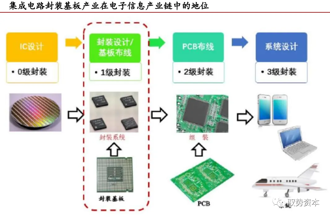
In electronic packaging engineering, electronic substrates (PCBs) can be used at different levels of electronic packaging (mainly for levels 2-5 of 1-3 level packaging), but packaging substrates are used for levels 2 and 3 of 1-2 level packaging, while ordinary PCBs are used for levels 3-5 of 2-3 level packaging. However, they all provide interconnection, protection, support, heat dissipation, assembly, and other functions for electronic components, aiming to achieve multi-pin integration, reduce the size of packaging products, improve electrical performance and heat dissipation, enable ultra-high density or multi-chip modularization, and ensure high reliability.
Motherboards (main boards), sub-boards, and carrier boards (substrate-like boards) of conventional PCBs (mostly motherboards, sub-boards, backplanes, etc.) are mainly used for levels 3-5 of 2-3 level packaging. They carry active devices like LSI, IC, and passive discrete components, interconnecting to form unit electronic circuits and perform their circuit functions.
With the continuous advancement and development of electronic installation technology, the boundaries between various levels of electronic installation are becoming increasingly blurred, with crossovers and integrations among the levels. In this process, the role of PCB is becoming more and more important, posing higher and newer requirements for PCB and its substrate materials in terms of functionality and performance.
The Process and Reasons for the Separation of Packaging Substrates from PCBs
After the 1980s, the widespread application of new materials and new equipment, along with the rapid development of integrated circuit design and manufacturing technology according to “Moore’s Law”, led to the emergence of small and sensitive semiconductor components, and large-scale integrated circuits and ultra-large-scale integrated circuit designs appeared, giving rise to high-density multi-layer packaging substrates. This caused integrated circuit packaging substrates to separate from ordinary printed circuit boards, forming proprietary manufacturing technology for integrated circuit packaging substrates.
Currently, in the mainstream products of conventional PCB boards, products with line width/spacing of 50μm/50μm are considered high-end PCB products, but this technology still cannot meet the technical requirements of currently mainstream chip packaging. In the field of packaging substrate manufacturing, products with line width/spacing of 25μm/25μm have become standard products, reflecting that the manufacturing technology of packaging substrates is more advanced than that of conventional PCBs. The fundamental reasons for the separation of packaging substrates from conventional printed circuit boards are twofold: on one hand, the refinement development speed of PCB boards is lower than that of chips, making direct connections between chips and PCBs relatively difficult. On the other hand, the cost of overall refinement improvement of PCB boards is much higher than the cost of interconnecting PCBs and chips through packaging substrates.
Main Structures and Production Technologies of Packaging Substrates
Currently, there is no unified classification standard in the packaging substrate industry. Usually, classification is done based on the substrate materials suitable for substrate manufacturing, production technology, etc. Based on different substrate materials, packaging substrates can be divided into inorganic packaging substrates and organic packaging substrates. Inorganic packaging substrates mainly include: ceramic-based packaging substrates and glass-based packaging substrates. Organic packaging substrates mainly include: phenolic-based packaging substrates, polyester-based packaging substrates, and epoxy resin-based packaging substrates, etc. Based on different manufacturing methods, packaging substrates can be divided into core (Core) packaging substrates and new coreless (Coreless) packaging substrates.
Core and Coreless Packaging Substrates
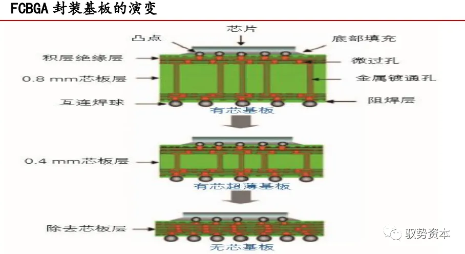
Core packaging substrates are mainly divided into two parts structurally, with the middle part being the core board and the upper and lower parts being the laminated boards. The manufacturing technology of core packaging substrates is based on high-density interconnection (HDI) printed circuit board manufacturing technology and its improved techniques.
Coreless substrates, also known as coreless boards, refer to packaging substrates that have had their core board removed. The new coreless packaging substrate is mainly produced by bottom-up electro-deposition technology to create interlayer conductive structures—copper pillars. It only uses insulating layers (Build-up Layer) and copper layers to achieve high-density wiring through semi-additive (SemiAdditive Process, abbreviated as SAP) lamination technology.
Advantages and Disadvantages of Coreless Packaging Substrates
-
-
Reduced electrical transmission path, further reduced AC impedance, and effective avoidance of echo loss caused by traditional core substrates’ PTH (plated through holes), which reduces the inductance of power system circuits and improves transmission characteristics, especially frequency characteristics;
-
Direct signal transmission can be achieved, as all wiring layers can serve as signal layers, thus improving wiring freedom and achieving high-density wiring, reducing the limitations of C4 layout;
-
Except for some processes, original production equipment can be used, and the number of process steps is reduced.
-
No core board support, coreless substrate manufacturing is prone to warping and deformation, which is currently the most common and significant problem;
-
Laminated boards are prone to breakage;
-
Some new equipment for semiconductor packaging coreless substrates needs to be introduced. Therefore, the challenges of semiconductor packaging coreless substrates mainly lie in materials and processes.
Statement: This article is copyrighted by the original author and does not represent the views of the association. The articles promoted by the “Jiangxi Province Electronic Circuit Industry Association” are only for sharing purposes and do not represent the stance of this account. If there are copyright issues, please contact us for deletion.