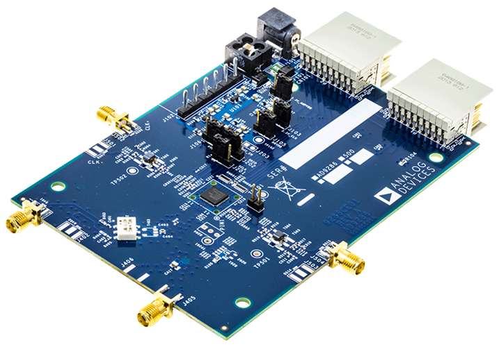
Overview
In the design of high-speed analog signal chains, the layout and routing of the printed circuit board (PCB) need to consider many options, some of which are more important than others, while others depend on the application. The final answers vary, but in all cases, design engineers should consider the overall picture rather than obsessing over every detail of the layout and routing. In many cases, it is impossible to cover everything, and trade-offs must be made based on the area of the circuit board and product.
Let’s share some important issues in ADC/DAC circuit and PCB design:
1
The Issue of Separating Digital Ground and Analog Ground
The simple answer is: it depends. The detailed answer is: usually, do not separate. Why not? Because in most cases, blindly separating the ground planes only increases the inductance of the return path, and the disadvantages outweigh the benefits.
From the formula V = L(di/dt), it can be seen that compromising the integrity of GND increases voltage noise as inductance increases. As inductance increases, the PDN impedance that designers strive to minimize also increases. With the growing demand for higher ADC sampling rates, there are very limited ways to reduce the switching current (di/dt). Therefore, unless it is necessary to separate the ground planes, please keep these grounds connected. Thus, our conclusion is that in most cases, we recommend against separating DGND and AGND, which contradicts early experiences.
Most of our products have size requirements, and there may not be enough and ideal space.
Due to space constraints, when the PCB cannot achieve good layout separation, it is necessary to separate the ground planes. This may be to meet traditional design requirements or sizes, necessitating placing noisy power buses or high-noise digital circuits in certain areas. In this case, separating ground planes is key to achieving good performance. However, for the overall design to be effective, these ground planes must be connected somewhere on the PCB via a ferrite bead or local connection point.
Ultimately, there will often be a connection point on the PCB that becomes the best position for return current to flow without degrading performance or forcing return current to couple to sensitive circuits. If this connection point is located near or below the converter, there is no need to separate the ground.
2
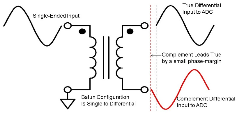
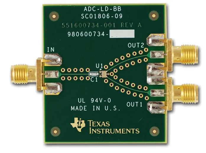
Selection of Baluns: Specifications and Types

3
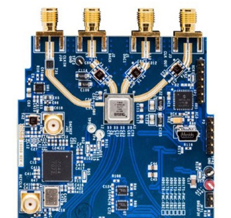
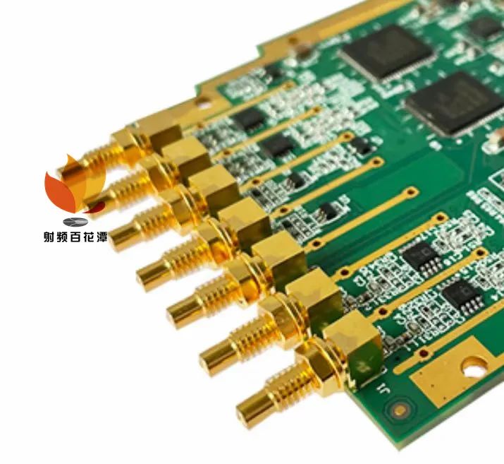
Selection of SMA Connectors
The vast majority of ADCs/DACs can use standard SMA connectors. If considering performance above 3G, it is necessary to perform matching simulation on the SMA connection to the PCB or switch to more advanced RF connectors; the matching of the connectors is also very important as it directly affects signal loss.
4
Selection of PCB Materials
5
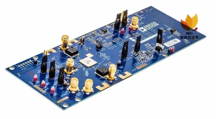
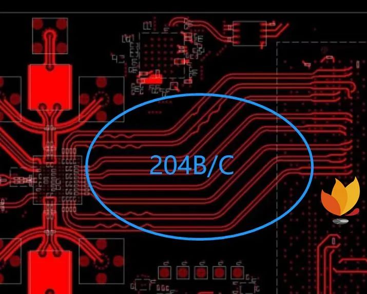
High-Speed Routing of JESD204B/204C
The connection between the analog world and the digital world relies on ADCs and DACs. With the increasing demand for data and the scarcity of spectrum resources, many industries’ data-intensive applications continue to push the boundaries of analog-to-digital data interaction. High-speed ADCs/DACs, as well as FPGA platforms suitable for processing large data, are gradually being developed. The JESD204 protocol for high bandwidth and high-speed analog-to-digital and digital-to-analog data transmission has also emerged. The protocol currently has several versions: JESD204A, B, and C. Compared to traditional LVDS transmission methods, it has higher link rates while saving IO counts.
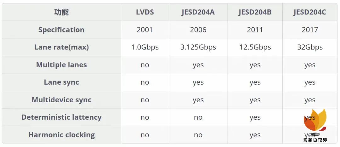
To meet the demand for faster data processing in data-intensive applications in the coming years, JESD204C defines multi-gigabit interfaces as essential communication channels between data converters and logic devices. Channel rates of up to 32 GSPS and 64b/66b encoding allow ultra-high bandwidth applications to improve system efficiency with minimal overhead. These and other standard improvements greatly benefit 5G communications, radar, and electronic warfare applications.
Typical chips supporting these protocols include: AD9081, AD9082, AD9988, AD9986, AD9177.
The JESD204C link protocol has reached a maximum single-channel rate of 32 Gbps, which requires good high-speed design experience and even simulation optimization of routing and vias to achieve the desired performance.
6
The Issue of Isolation
7
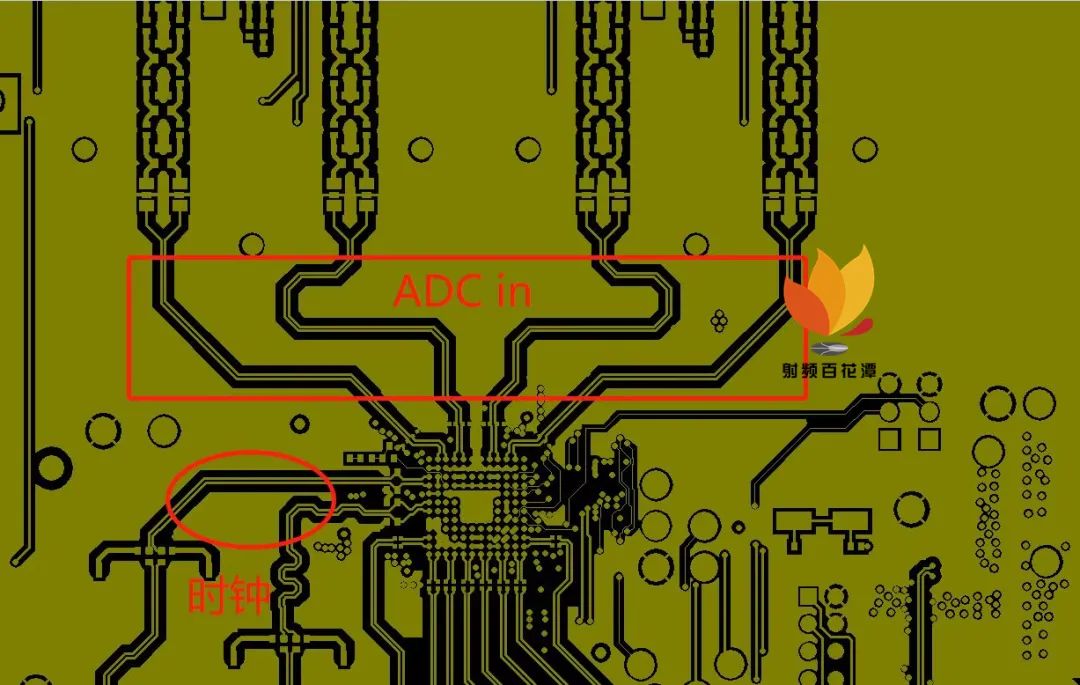
The Issue of Clock Interference
Scan QR Code to Contact