Advertisement Divider
PCB Network City News

Professor Bai Rongsheng is well-known in the industry and has been writing articles related to circuit boards and their upstream and downstream since 1988. He has published more than ten professional books, including “Comprehensive Guide to PCB Wet Processing”, “PCB and Lead-Free Soldering”, “PCB Terminology Manual”, and “PCB Terminology Manual – Basic Edition”. He has extensive experience in failure analysis of electronic components and has analyzed the causes and countermeasures based on real cases to improve product reliability.
Moreover, Professor Bai has unique insights into the technical fields of the upstream and downstream supply chain in the PCB industry. For decades, he has personally engaged in research and writing without any slack.
Starting today, PCB Network City will successively share Professor Bai’s expert technical articles published in the “Printed Circuit Information” magazine to help colleagues in the industry.
This article is from the “Expert Forum” section of the “Printed Circuit Information” (January 2023 issue), titled “5G Strong Demand PCB Phenomenon Unprecedented (6) – Disassembly and Analysis of iPhone 12”. Unauthorized reproduction by any individual or organization is prohibited. If reproduction is required, please contact the backend for permission. Thank you!
The iPhone series has been utilizing TSMC’s chip manufacturing and packaging since the iPhone 7, replacing the original 6-layer substrates with RDL and achieving great success. This article will explain the selection of ten-layer and eight-layer boards and their components.
I. Introduction
The iPhone series has been utilizing TSMC’s chip manufacturing and packaging since the iPhone 7, replacing the original 6-layer substrates with RDL and achieving great success. Starting from the tenth generation iPhone, the original ten-layer motherboard has been halved and soldered into a thicker twenty-layer board, aiming to save space for a larger battery to extend battery life. This twenty-layer motherboard is made up of three single boards stacked together, showcasing an unprecedented intricate layout and complexity. TPCA purchased four standard models of the iPhone 12 for 27,000 yuan, and from the logo ‘AM’ marked on the motherboard, it can be seen that it is the ten-layer and eight-layer boards shipped from the Hong Kong company OPC Meiwei in Guangzhou. Meiwei was sold to the American company TTM in 2010 and then sold to the Japanese company Asahi Kasei Microdevices in 2020. Currently, Meiwei is registered under UL as AKM MEADVILLE. The following is the outline of this article.
II. Overall Appearance and Sampling of the iPhone 12
III. Description of the First Sampling of the Mainboard No. 1
IV. Description of the Second Sampling of the Mainboard No. 2
V. Content of the Third and Fourth Samplings
VI. Market for FOWLP and FOPLP
II. Overall Appearance and Sampling of the iPhone 12
2.1 iPhone 12 Overall and Mainboard
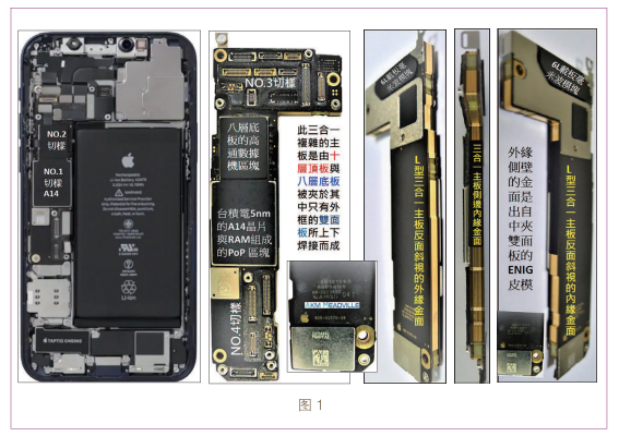
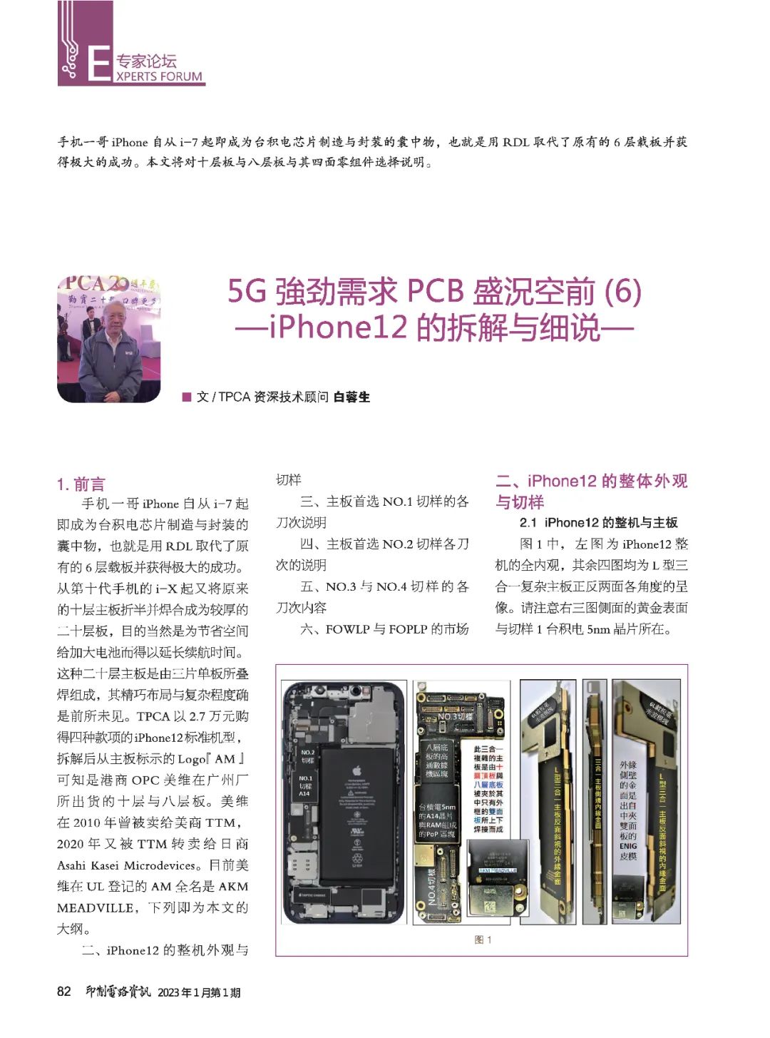
In Figure 1, the left image shows the full internal view of the iPhone 12, while the other four images present various angles of the L-shaped three-in-one complex motherboard from both sides. Please note the golden surface on the side of the right three images where the 5nm chip from TSMC is located.
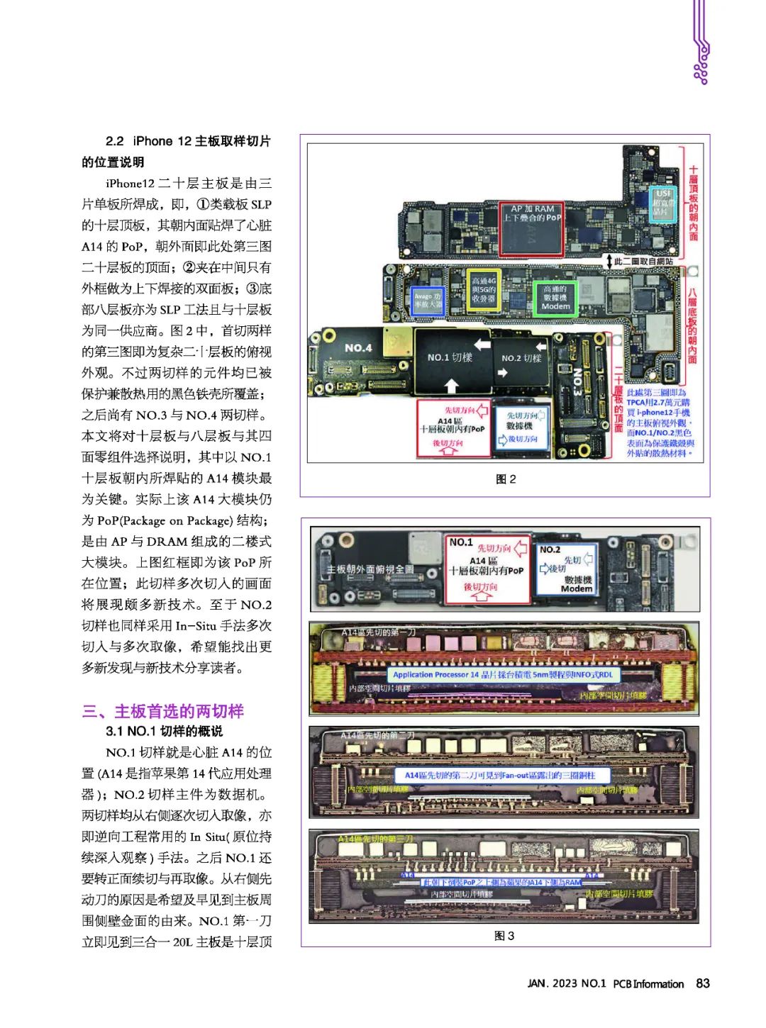
 2.2 Explanation of Sampling Positions on the iPhone 12 MainboardThe twenty-layer mainboard of the iPhone 12 is composed of three single boards. That is, ① the ten-layer top board of the SLP type, where the A14 PoP is soldered on the inner side, while the outer side is the top surface of the twenty-layer board in the third image; ② a double-sided board with only an outer frame for upper and lower soldering; ③ the eight-layer bottom board is also of the SLP method and from the same supplier as the ten-layer board. In Figure 2, the third image of the first two samplings shows the overhead view of the complex twenty-layer board. However, the components of both samples are covered by a black iron shell for protection and heat dissipation; there are still NO.3 and NO.4 samplings to follow. This article will explain the selection of the ten-layer and eight-layer boards and their four-sided components, with the NO.1 ten-layer board soldered to the critical A14 module on the inner side. In fact, this A14 large module is still a PoP (Package on Package) structure, consisting of an AP and a DRAM module. The red box in the above image shows the location of the PoP; this sampling with multiple cuts will reveal many new technologies. The NO.2 sampling also uses the In-Situ method for multiple cuts and multiple images, hoping to find more new discoveries and share new technologies with readers.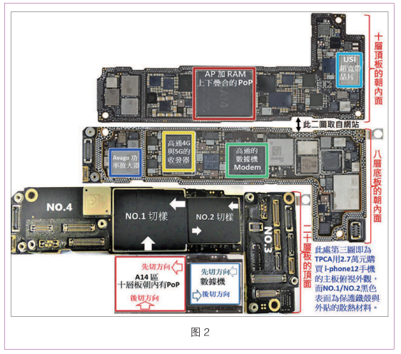
III. The Two Main Sampling Selections
3.1 Overview of Sampling No. 1Sampling No. 1 is the position of the A14 heart (A14 refers to Apple’s 14th generation application processor); the main component of Sampling No. 2 is the data modem. Both samples are cut in from the right side sequentially, which is the In Situ method commonly used in reverse engineering. After that, NO.1 will also need to be cut from the front for further imaging. The reason for starting from the right side is to see the origin of the golden surface on the side walls of the motherboard as early as possible. The first cut of NO.1 immediately reveals that the three-in-one 20L motherboard is formed by soldering the ten-layer top board and the eight-layer bottom board with only the outer frame of the double-sided board. The double-sided board acts as an interposer. In Figure 3, the second cut of the third image shows the expected three circles of copper pillars in the A14 peripheral FO area; the third cut in the fourth image shows the PoP first floor 5nm A14 chip and the second floor dual-chip wire-bonded DRAM module.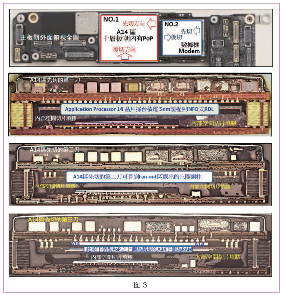
3.2 Presentation of the Right Cuts of Sampling No. 1
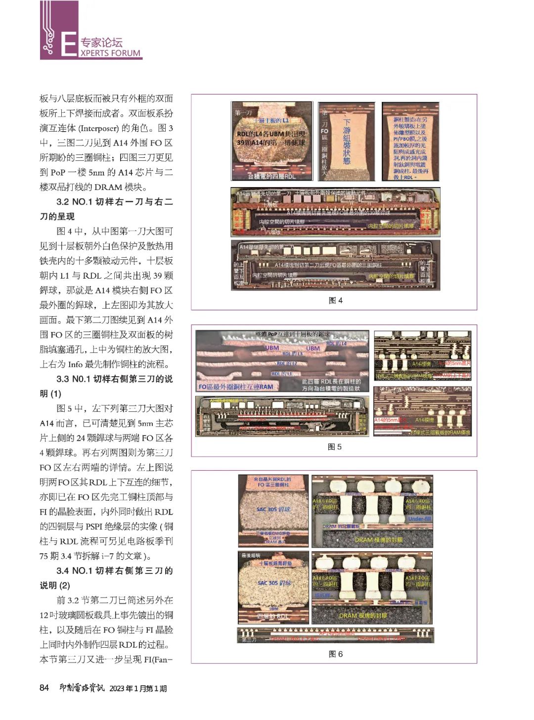
In Figure 4, the large image from the first cut in the middle shows more than ten passive components inside the white protective and heat-dissipating iron shell of the ten-layer board facing outward. The ten-layer board has 39 solder balls appearing between L1 and RDL on the inner side, which are the outermost solder balls in the FO area of the A14 module. The upper left image is an enlarged view of this. The second cut image below continues to show the three circles of copper pillars in the A14 peripheral FO area and the resin-filled vias of the double-sided board; the upper middle is a close-up of the copper pillars, and the upper right shows the process of making copper pillars by Info.
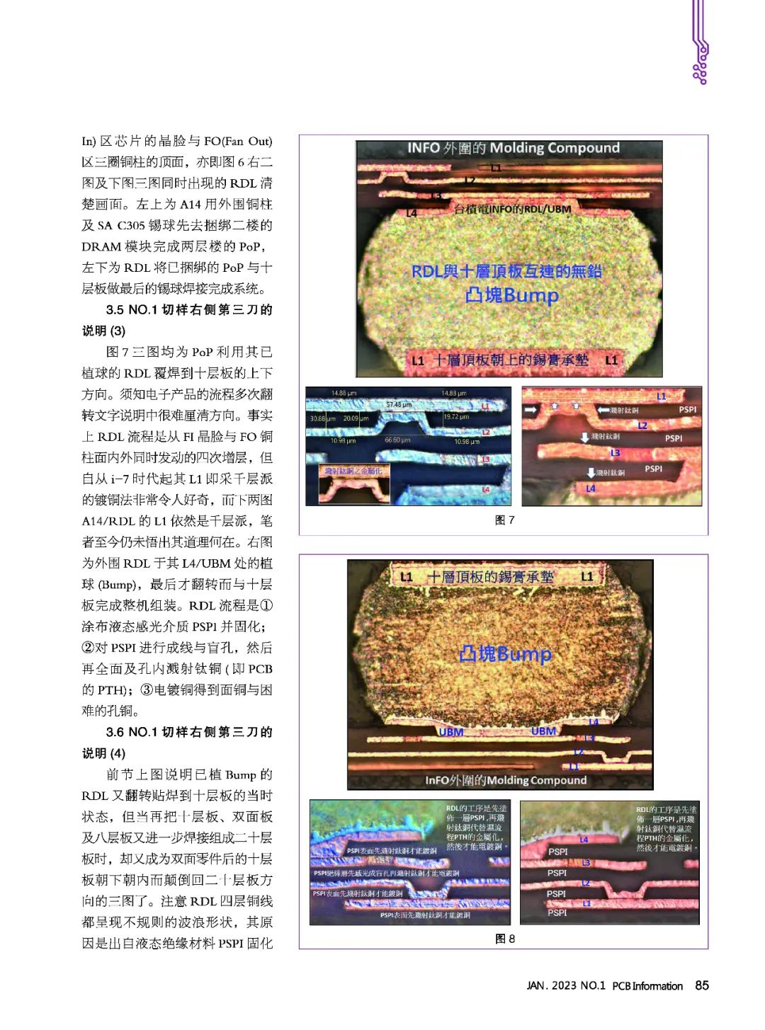
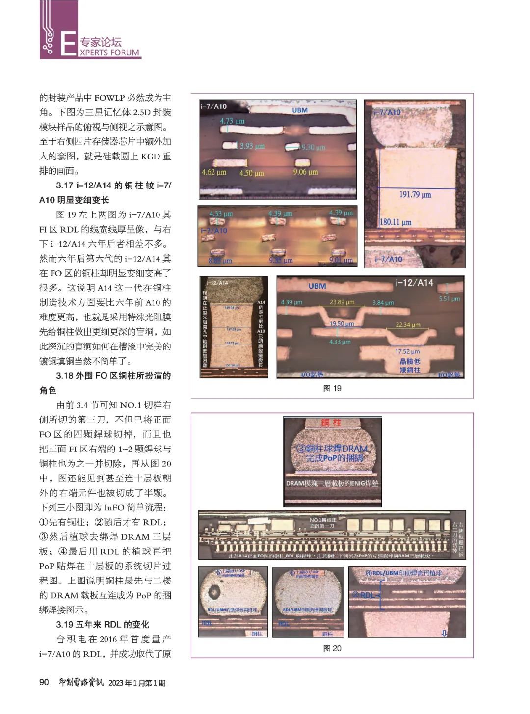
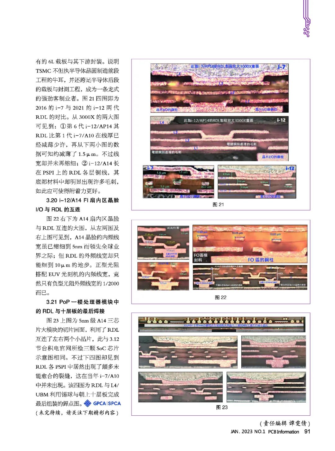
3.3 Explanation of the Right Third Cut of Sampling No. 1 (1)In Figure 5, the large image of the third cut clearly shows 24 solder balls on the upper side of the 5nm main chip for A14, along with four solder balls at each end of the FO area. The two images on the right show the details of the FO area at both ends of the third cut. The upper left image illustrates the details of the RDL interconnections between the upper and lower FO areas, that is, the completed copper pillar tops in the FO area and the chip surface of FI, where four copper layers and PSPI insulation layers are simultaneously made inside and outside (the copper pillar and RDL process can be seen in the PCB Quarterly issue 75, section 3.4, article on i-7 disassembly).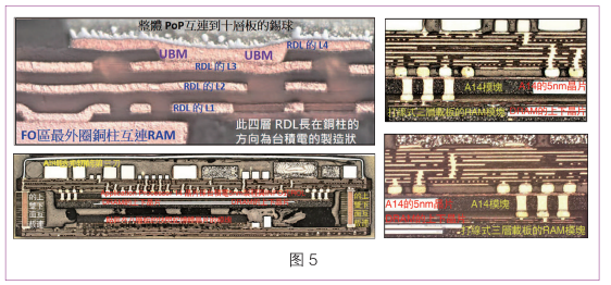 3.4 Explanation of the Right Third Cut of Sampling No. 1 (2)The previous section has briefly described the copper pillars pre-planted on a 12-inch glass wafer carrier, as well as the process of simultaneously making four layers of RDL on the FO copper pillars and the chip surface. This section’s third cut further presents the chip surface of the FI (Fan-In) area and the top surface of the three circles of copper pillars in the FO (Fan Out) area, as shown in the right second image and the lower third image simultaneously showing the clear RDL image. The upper left shows the peripheral copper pillars of A14 and the SA C305 solder balls used to bind the second floor DRAM module to complete the two-story PoP, while the left lower shows the final soldering of the bound PoP with the ten-layer board to complete the system.
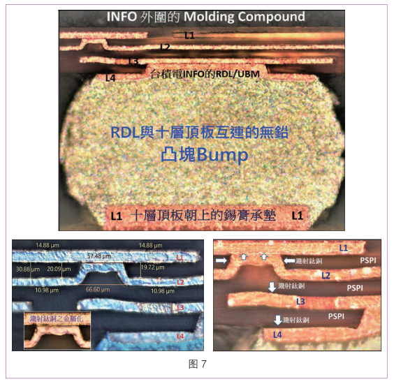
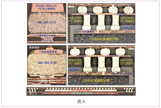 3.5 Explanation of the Right Third Cut of Sampling No. 1 (3)Figures 7 show the PoP utilizing its already implanted solder balls to solder onto the upper and lower directions of the ten-layer board. It should be noted that the process of electronic products often involves multiple flipping, making it difficult to clarify the direction in the text description. In fact, the RDL process is initiated simultaneously from the inner and outer surfaces of the FI chip and FO copper pillars in four increments. However, since the i-7 era, its L1 has adopted a multi-layer copper plating method, which is very intriguing, and the following images of A14/RDL’s L1 still follow this method; the author still has not figured out the reasoning behind it. The right image shows the peripheral RDL at its L4/UBM location where the bump is finally flipped and assembled with the ten-layer board.The RDL process includes: ① applying liquid photo-sensitive medium PSPI and curing it; ② forming lines and blind holes on PSPI, and then sputtering titanium-copper (which is PCB’s PTH); ③ electroplating copper to achieve surface copper and difficult hole copper.
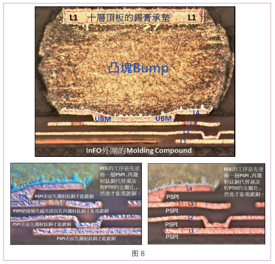
 3.6 Explanation of the Right Third Cut of Sampling No. 1 (4)The previous section’s images have shown that the RDL with bumps has been flipped and soldered onto the ten-layer board’s state at that time. However, when the ten-layer board, double-sided board, and eight-layer board are further soldered to form the twenty-layer board, it becomes the three images with the ten-layer board facing downward and inward, reversing back to the direction of the twenty-layer board. Note that the four layers of copper wires in the RDL show irregular wave shapes, which is due to the uneven surface of the cured liquid insulating material PSPI, but it does not excessively affect high-speed signal transmission; otherwise, how could it be mass-produced and used smoothly by users over the long term? (Note: InFO is the abbreviation for TSMC’s Integrated Fan-Out patent, also known as InFOWLP; PSPI refers to Photo-Sensitive Polyimide insulation material).(Figure 8)
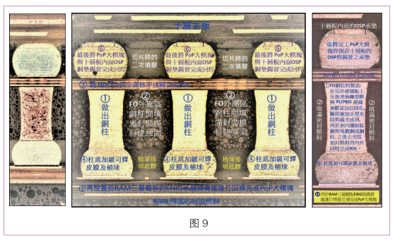
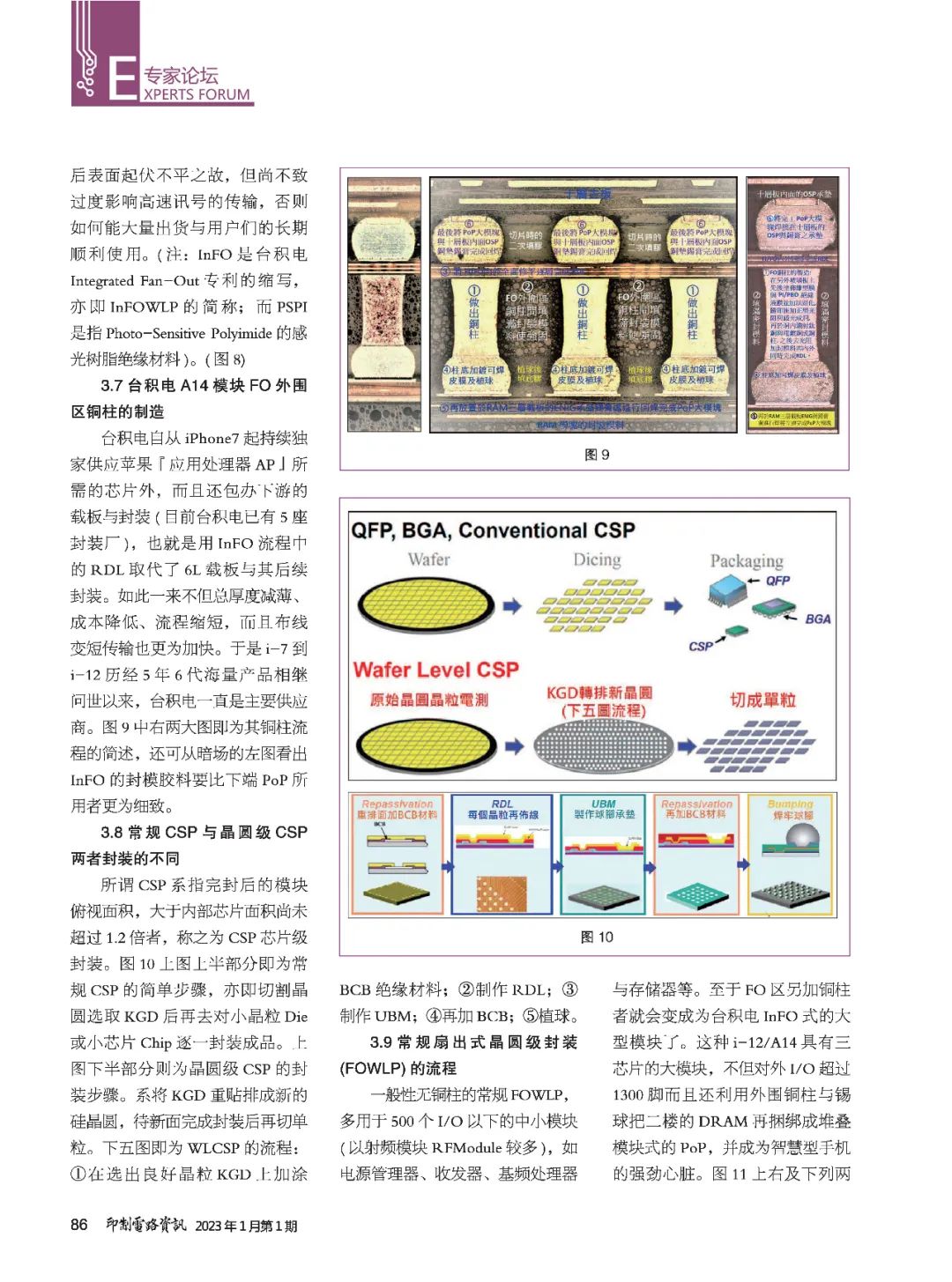
 3.7 Manufacturing of TSMC’s A14 Module FO Peripheral Copper PillarsSince the iPhone 7, TSMC has continued to exclusively supply the chips required for Apple’s “Application Processor AP”, as well as handling the downstream substrate and packaging (currently TSMC has five packaging plants), replacing the 6L substrate and subsequent packaging with RDL in the InFO process. This not only reduces the overall thickness, lowers costs, and shortens processes, but also shortens wiring for faster transmission. Thus, from the i-7 to i-12, five years and six generations of massive products have been successively launched, with TSMC being the main supplier. In Figure 9, the two large images on the right summarize the copper pillar process, and the left image in the dark field shows that the molding glue used in InFO is more refined than that used in the lower PoP.
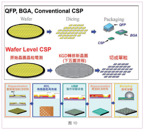
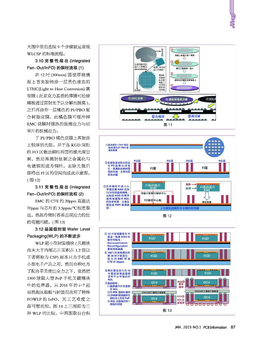
3.8 Differences Between Conventional CSP and Wafer-Level CSP PackagingThe so-called CSP refers to the module’s top view area after complete packaging, which is greater than the internal chip area but does not exceed 1.2 times, referred to as CSP chip-level packaging. The upper half of the upper part of Figure 10 shows the simple steps of conventional CSP, which involves cutting the wafer to select KGD and then packaging each small die or chip individually. The lower half of the image shows the packaging steps of wafer-level CSP, which involves re-stacking KGD into a new silicon wafer and cutting individual units after the new surface is completed. The following five images illustrate the WLCSP process: ① applying BCB insulation material to selected good die KGD; ② making RDL; ③ making UBM; ④ applying BCB again; ⑤ bumping.
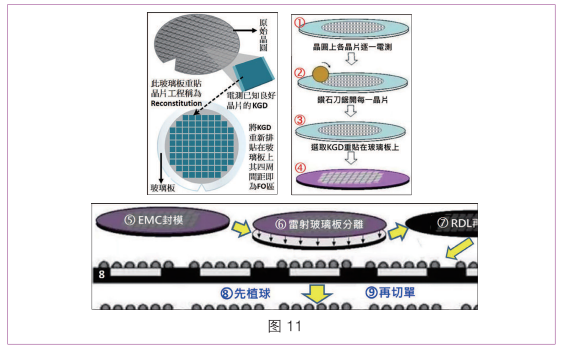
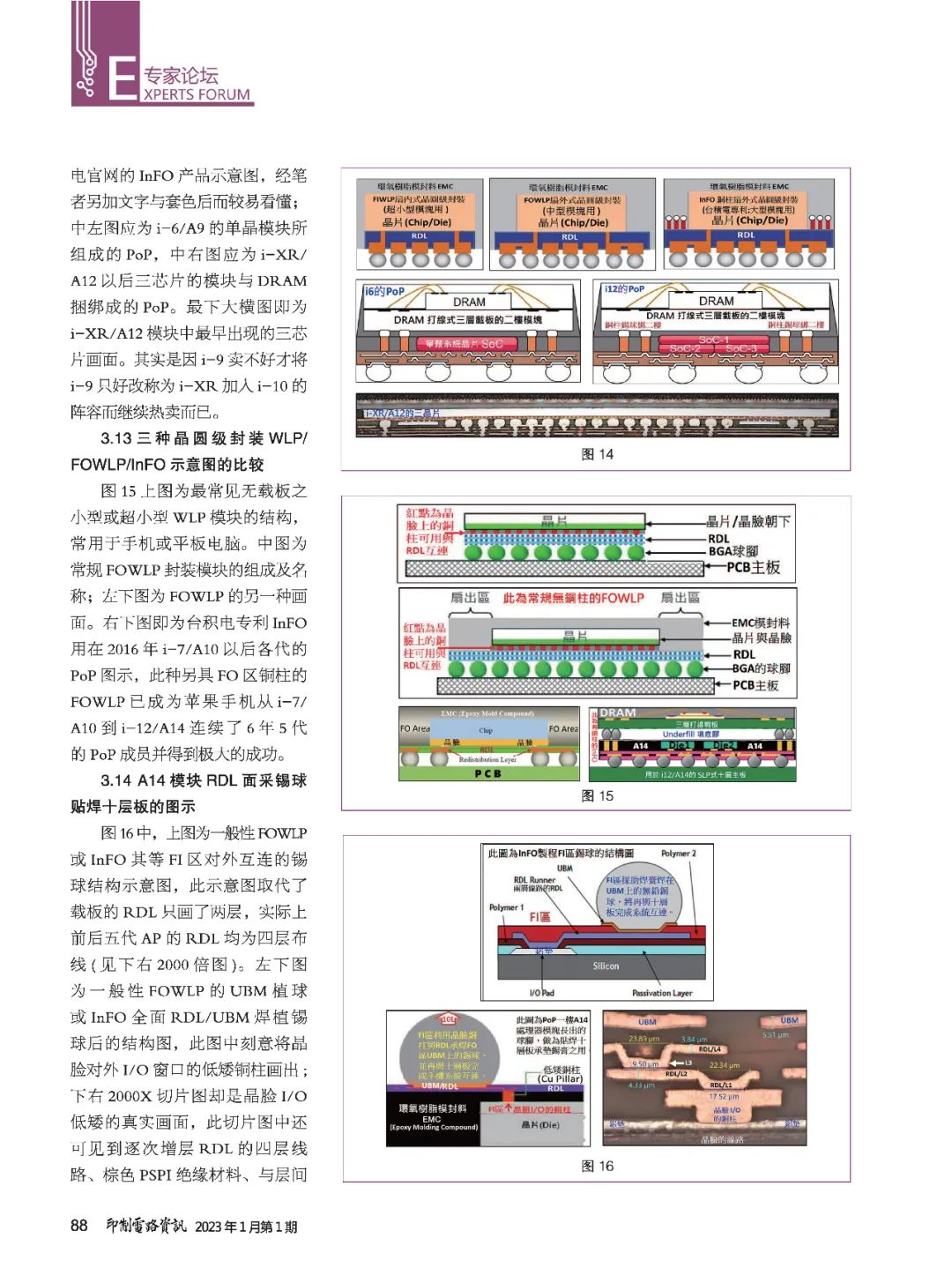
3.9 Process of Conventional Fan-Out Wafer-Level Packaging (FOWLP)Generally, conventional FOWLP without copper pillars is mostly used for medium and small modules with less than 500 I/O (mostly RF modules), such as power managers, transceivers, baseband processors, and memory. If the FO area adds copper pillars, it becomes TSMC’s InFO-style large module. This i-12/A14 large module, which has three chips, not only exceeds 1300 I/O but also uses peripheral copper pillars and solder balls to bind the second floor DRAM into a stacked module PoP, becoming the powerful heart of smart phones. The two large images in the front and back of Figure 11 show the standard process of conventional WLCSP in nine consecutive steps.
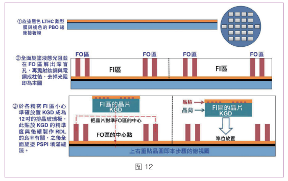
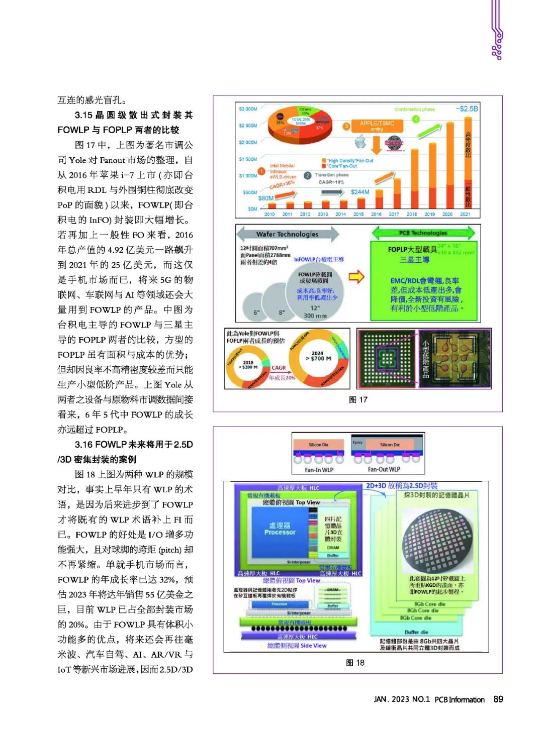
3.10 Copper Pillar Process of Integrated Fan-Out (InFO)On a 12-inch (300mm) round thick glass plate, a layer of black liquid LTHC (Light to Heat Conversion) release film is first spun coated (this acrylic-based thin film can be decomposed and removed through laser light passing through the glass plate), followed by a layer of orange PI/PBO composite resin film, which can buffer the thermal expansion stress during EMC pouring and the mechanical stress of cutting single pieces. A thicker photoresist is then spun on the PI/PBO orange film, and then the required photo-sensitive deep blind holes for copper pillars are made in the FO area of each KGD spacing, followed by titanium-copper metallization and copper electroplating to form copper pillars. After removing the photoresist, the space of the FI area is obtained, as shown in this illustration.(Figure 12)
For more content, scroll down to view the images below

Advertisement Divider