Follow and star our public account for exciting content delivered daily.

Source: Online materials
We are still debugging an image issue where one chip exhibits a flickering phenomenon in the output image.
The system is initially defined as follows:
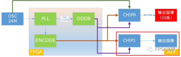
Explanation:
(1) A 24MHz crystal oscillator outputs a clock that is fed into the FPGA and also into CHIP0 as its working clock (green line);
(2) The FPGA receives the 24M clock and outputs 36MHz and 74.25MHz through the PLL as logic clocks, encoding the video stream data through the ENCODE module, outputting 8/16 bits of parallel data to the port (gray line);
(3) The clock associated with the data is output from the pins via ODDR;
(4) CHIP0 and CHIP1 receive the same clock and data, with the difference being that CHIP0 is a self-developed chip with lower fault tolerance than CHIP1.
The phenomenon is that CHIP1 can decode and output the image normally, while CHIP0 exhibits flickering in the output image.
Since the design team for CHIP0 confirmed that the working clock and the associated clock must be sourced from the same origin, the FPGA was designed with this scheme, using a single 24M crystal oscillator, supporting two modes for image output: 1) 36M associated clock and data, with normal image display; 2) 74.25M associated clock and data, resulting in flickering output.
Debugging approach:
A. Encoding issue: This can be largely ruled out since CHIP1 can decode and display the image normally, and the decoding status register of CHIP0 shows normal decoding;
B. Clock issue: Hardware measurements of the clock show that both the 24M working clock and the 74.25M and 36M associated clocks are stable, with frequency offsets of 3-13 ppm, which meets hardware requirements;
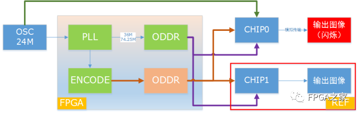
C. Phase issue: This refers to the phase relationship between the output clock and data. Since the chip samples on the rising edge, to ensure correct sampling, I added ODDR to the original data path to reduce issues caused by layout and routing anomalies due to resource constraints, as shown below:
According to the input-output timing relationship of the XILINX ODDR primitive:
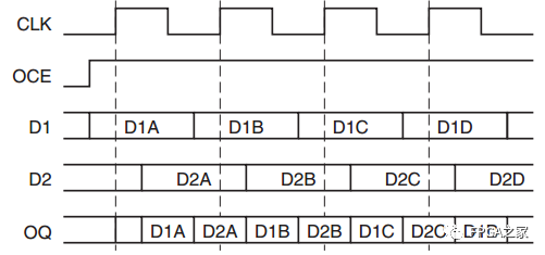
By initializing the input and output clocks to D1(0) and D2(1), it can generally be ensured that data is sampled on the rising edge. However, after modifications, the image still flickers.
At this point, I collaborated with the chip design team to see if we could identify the issue by reading and writing the status registers.
CHIP0 can be roughly divided into two parts according to my preliminary understanding: decoding and display, as shown below:
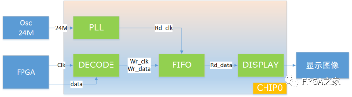
The decoding uses the input associated clock to sample and decode the data, writing the data into FIFO. The input working clock generates the read FIFO clock, sending the read data to the DISPLAY module for output and display.
By reading and writing the registers, it was found that the DECODE module’s status register was always normal, while the display module’s status register was abnormal. Further investigation revealed that there was an empty read issue with the FIFO, meaning it was writing slowly while reading quickly. From the chip’s perspective, with normal decoding and clock, there should not be any FIFO empty/full errors.
At this point, I checked the FPGA output clock again through the PLL core and found that the clock output from the FPGA was not 74.25M, but rather 74M (which was misleadingly measured as stable at 74.25M by hardware).
This is because the FPGA PLL cannot generate arbitrary clocks without deviation. Under the currently selected device, if a 24M crystal oscillator is used as input, the output clock of 74.25M can only actually be 74M, while the 24M clock can generate a stable 36M clock; if a 27M crystal oscillator is used, it can output a stable 74.25M clock but cannot output a stable 36M clock, resulting in 36.033M. Thus, it can be analyzed that the video stream generated at 74M is actually slightly less than 30 frames (25 frames), while the chip uses a fixed 30 frames (25 frames) for reading, and since the chip has high requirements for frequency and frame rate matching on both ends, this could indeed cause an empty read phenomenon. CHIP1 can work normally likely due to its better fault tolerance, which can correct the frequency offset or frame rate difference on both ends.
To accommodate both output modes, the clock scheme was modified as follows:
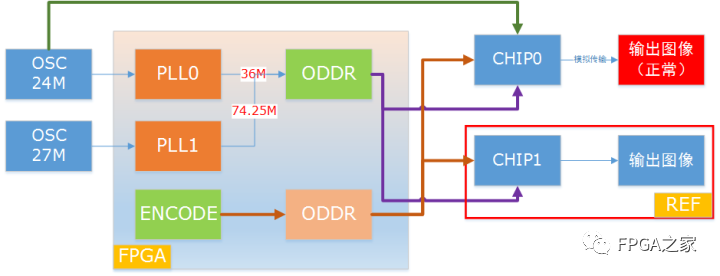
Using two crystal oscillators, one at 24M and the other at 27M, the FPGA internally uses two PLLs, with PLL0 generating the 36M clock and PLL1 generating the 74.25M clock. At this point, reading the status registers of the chip shows normal operation, and images can be displayed correctly in both modes.
Summary:
(1) For the input-output clock frequencies of the FPGA’s internal PLL, as long as we set the frequency, phase, duty cycle, and other parameters correctly, it generally works stably. However, for some external devices with poor fault tolerance to frequency offsets, even a slight frequency deviation can cause the chip to malfunction, which needs to be noted;
(2) Theoretically, there should not be a special relationship between the chip’s working clock and sampling clock, such as the requirement for the same source in this case. If the same source is required, the accuracy of the associated clock should be confirmed first in cases where normal operation cannot be achieved.
(End of full text)

Want to learn about FPGA? Here are some example shares, ZYNQ design, follow our public account to explore.