“NOR flash memory has reached its limits and cannot be compatible with processes below 28 nanometers (nm).” A few years ago, industry giants, including Infineon, reached this conclusion regarding the limits of embedded NOR Flash technology. Infineon even developed ferroelectric random access memory (FRAM) to prove its viability as an alternative to NOR flash memory.
However, a domestic startup established less than five years ago—Ningbo Lingkai Semiconductor Technology Co., Ltd. (hereinafter referred to as “Lingkai Semiconductor”)—has broken this conclusion with its innovative technical architecture. This not only extends the life of NOR Flash technology but also opens up new opportunities for innovative applications of embedded flash memory in the AI era. Founded by Mr. Jin Bo, a senior expert with thirty years of experience in the semiconductor industry and a Silicon Valley technology leader, Lingkai Semiconductor’s core technology, ATopFlash©, is key to overcoming the industry’s recognized challenge that NOR Flash cannot achieve further breakthroughs in advanced logic process nodes of 28nm and below. The emergence of this technology not only addresses the existence of memory below 28nm but also offers significant cost competitiveness due to its small unit area.

Mr. Jin Bo, Founder and CEO of Lingkai Semiconductor
Previously, due to the lack of mature solutions for traditional embedded NOR Flash below 28nm, systems often relied on external storage, leading to increased complexity and limited performance. ATopFlash© solves this global bottleneck through its unique technical path, providing critical storage support for SoC/MCU to evolve towards more advanced processes. Recently, “Electronic Engineering Magazine” interviewed Mr. Jin Bo to detail the technical origins, competitive advantages of ATopFlash©, and how architectural innovation empowers embedded NOR Flash to become the core storage medium for MCU and SoC systems.

Breaking Through the Traditional Floating Gate Technology with a “New Technical Path”
NOR Flash technology, as a non-volatile memory, has played a critical role in various fields since its inception in the 1980s, thanks to its unique characteristics (especially supporting chip-in-execution XIP, allowing programs to run directly without first loading into RAM). This feature makes it particularly suitable for storing boot code, operating system kernels, critical program code, and configuration data.
However, several years ago, 45nm was widely regarded as the last technology node for NOR Flash. In particular, traditional NOR Flash based on ETOX floating gate technology has no design space below 45nm, reaching physical limits and causing stagnation in industry technological progress for many years.
Faced with the global industry’s dilemma, Mr. Jin Bo saw an opportunity for Lingkai Semiconductor. This determination and confidence stem from his comprehensive management, technical development, and production operation experience in the NOR Flash field for thirty years.
As early as 1995, Mr. Jin joined the multinational semiconductor company Cypress in Silicon Valley. During his 18 years there, he grew from a technical development engineer to a business unit leader and even a company executive. During this time, he not only invented the general architecture of 6T cell SRAM for embedded applications below 65nm and the mainstream SONOS NOR Flash 2T cell architecture but also assisted Huahong NEC and Huali Semiconductor in overcoming technical and operational challenges to achieve business upgrades.
After leaving Cypress, Mr. Jin served as the president of the domestic listed company Juchen Semiconductor, pioneering global new applications of EEPROM in mobile camera modules and Bluetooth, helping the company rise from fourth in China to first in the Asia-Pacific region.
With a solid technical foundation and rich management experience, Mr. Jin developed the ATopFlash© technology through architectural innovation in less than five years since founding Lingkai Semiconductor, despite the industry’s belief that NOR Flash was difficult to break through.
Of course, the ATopFlash© technology breaks through the physical limits of traditional floating gate/ETOX technology and provides a new technical path, which has a little “story”: During his time at Cypress, Mr. Jin promoted the licensing of embedded NOR Flash (SONOS 2T1b) 0.13-micron technology to Huahong NEC, establishing a telecom card foundry business and supporting four domestic chip design companies, including Datang Microelectronics, Tsinghua Tongfang, Huada Microelectronics, and Nanhua Hong, breaking Samsung’s 95% market monopoly at the time. Samsung quickly responded by upgrading to 90nm technology, nullifying Huahong NEC’s cost advantage. Due to the limitations of Huahong NEC’s factory equipment, upgrading the process was not feasible, and Mr. Jin subsequently conceived an innovative architecture that halved the chip area, once again helping them defeat Samsung.
The ATopFlash© technology is also an innovative architecture and an important invention by Mr. Jin after returning to his roots, allowing NOR Flash technology to be revived and continue to iterate.

Architectural Innovation Breaks the “Ceiling” of 28nm NOR Flash
The implementation of ATopFlash© technology relies on another key figure behind Lingkai Semiconductor. He began researching charge trap physical mechanisms during his doctoral studies and has over 20 years of deep accumulation, having led a domestic storage giant to achieve a world-leading breakthrough in 232-layer 3D NAND technology. The charge trap mechanism is the core of ATopFlash© technology. After completing the concept, Mr. Jin immediately invited this former Cypress colleague to evaluate the technical feasibility. After receiving high praise for being “unpretentious, practical, and easy to mass-produce, clearly an expert,” Mr. Jin’s confidence soared. With his support, Lingkai Semiconductor successfully completed the 55nm chip technology verification based on the ATopFlash© architecture in May 2025, aiming to achieve new product tape-out in the second half of this year.
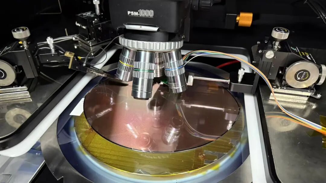
Traditional NOR Flash uses floating gate technology to store charge, but faces issues such as uncontrolled tunneling oxide layer barriers, inter-cell crosstalk, and difficulties in increasing storage density at nodes below 28nm. Floating gate technology (currently the mainstream solution) struggles with multi-bit storage due to random charge distribution, limited cell density, and requires complex patterning processes and numerous photomask layers (approximately 30 layers). Even TSMC’s floating gate-based 28nm NOR Flash chip has a die size of 0.043μm² but requires additional dozens of photomask layers, making it extremely cost-ineffective.
In short, 28nm has become the technical ceiling for traditional floating gate NOR, with the fundamental contradiction being that miniaturization requires more precise charge control, but quantum effects exacerbate instability. ATopFlash© technology abandons traditional floating gate design and instead adopts the charge trap technology that has matured in 3D NAND production. Its charge trap layer (such as silicon nitride) has stronger charge confinement and better miniaturization potential, fundamentally enhancing the reliability and scalability of storage cells, allowing for a 50% reduction in cell area. At the same time, the number of photomask layers required in the manufacturing process is reduced by nearly 30%, requiring only 22-23 layers. This means that more chip dies can be produced from a single wafer, significantly lowering unit costs and forming core market competitiveness.
It is worth mentioning that based on ATopFlash© technology, embedded NOR Flash has advanced to the 40nm logic process node. Mr. Jin introduced that the 40nm E-Flash technology (cell size=0.045μm²) has already been validated in product chips.
In addition to the charge trap mechanism, another core innovation of ATopFlash© technology is the “dual storage group pairing” design, as the full English name of this technical architecture suggests—Advanced Technology of Paired Flash. Through unique circuit layout and cell structure, it achieves multiple performance improvements and cost advantages.
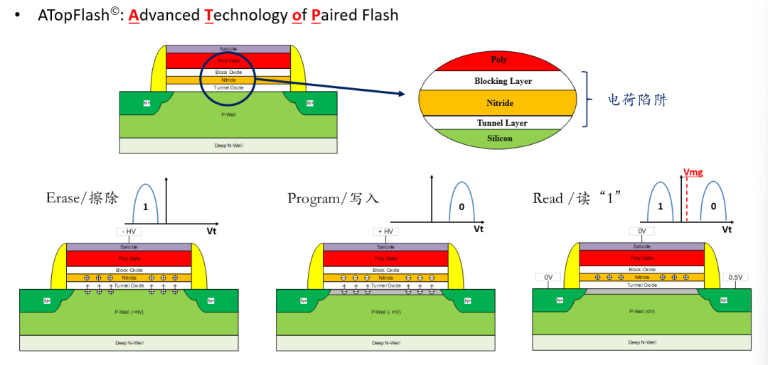
Currently, there are only a few global NOR Flash manufacturers using charge trap technology, including Cypress, Puran, and Lingkai Semiconductor. Puran’s SONOS 2T1b technology architecture is licensed from Cypress.
Mr. Jin compared the ATopFlash© technology architecture with the existing Cypress SONOS 2T1b architecture, and found that ATopFlash© has significant advantages in many aspects:
-
Smaller cells: ATopFlash© is smaller than 1T1b, eliminating the high-voltage NMOS selection transistor that is not conducive to miniaturization.
-
Fewer photomask layers: Saves one metal photolithography layer required for the common source line.
-
Simplified process: Reduces the photolithography layers and process steps required to form the selection NMOS, making the process more unified and straightforward.
-
Higher read current: Read current increases by >50%.
-
Improved reliability: Completely avoids potential SG leakage/reliability issues during programming operations.
-
Better miniaturization path: The further miniaturization path of ATopFlash© technology can foreseeably reach FinFET 5nm.
This means that ATopFlash© technology can be fully compatible with existing logic chip processes, empowering third-party mass production of 40/28/22nm SoC/MCU, and will also adapt to FinFET 14/10/7/5nm logic processes in the future.

Building a “Technical Moat” for eFlash
Previously, the industry believed that emerging memories such as MRAM (magnetoresistive random access memory) and RRAM (resistive random access memory) might replace NOR Flash in specific scenarios. In particular, TSMC and Infineon have been collaborating on RRAM technology since 2010, aiming to address the limitations of traditional embedded flash memory (eFlash) in performance, power consumption, and cost. This further reinforced the consensus that “NOR flash cannot be compatible with processes below 28nm,” pushing the industry towards research on new memory technologies. However, despite the technical principles suggesting many advantages, the maturity and cost of new memory technologies make ATopFlash© technology a new choice.
Currently, MRAM is limited by material complexity (such as ferromagnetic layer CoFeB), density bottlenecks, and anti-magnetic interference designs, making its cost high and difficult to compete with NOR Flash in the short term. While RRAM has a lower cost, its read/write cycles (about 10,000 times) and extreme environmental reliability are slightly inferior to MRAM, making it more of a supplement to NOR Flash rather than a replacement.
Both MRAM and RRAM control and operate through current, and the industry’s technical accumulation time is relatively short, far less mature than NOR Flash. ATopFlash© technology, on the other hand, adopts a mature and stable threshold voltage control mode, reducing the complexity and risk of peripheral circuit design. Additionally, public data shows that although MRAM and RRAM have been trial-produced in more advanced logic processes such as 14nm and 22nm, their chip unit areas are very large. In contrast, ATopFlash© technology:
Can achieve a die unit area of 0.023μm² at 28nm process, almost equivalent to the die unit area of 0.022μm² achieved by RRAM at 14nm.
At 40nm process, the die unit area is 0.045μm², even better than MRAM’s 0.046μm² achieved at 22nm.
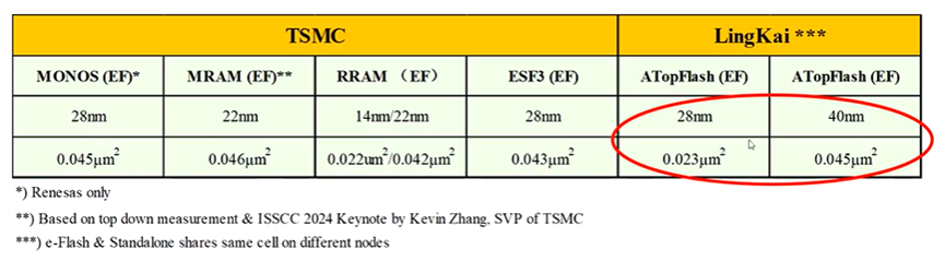
This indicates that ATopFlash© architecture innovation allows NOR Flash to lead MRAM and RRAM by more than a generation in logic processes, not considering the latter’s challenges in maturity and cost. Furthermore, ATopFlash© advantages also include the need to add only three layers of low-cost photomasks to achieve mass production of the process.
Regarding the prospects for technology adoption, Mr. Jin stated, “Many domestic chip design companies have used charge trap technology provided by wafer foundries, so they will not be unfamiliar with our technology. The physical mechanisms are similar, but our area is half smaller.” In his view, ATopFlash© technology will provide a general code storage solution for the embedded market that far exceeds traditional NOR Flash in terms of high performance and excellent cost-effectiveness.
Currently, Lingkai Semiconductor has established a disruptive, patent-protected underlying architecture innovation, building its own “technical moat.” Based on the ATopFlash© technology architecture, Lingkai Semiconductor has obtained 17 Chinese invention patents.

“Big Opportunities in a Niche Market”
Currently, NOR Flash is widely used in smart fields such as wearable devices, automotive electronics, and industrial control, but the market concentration is not high. Therefore, international memory giants are withdrawing from the mid-to-low-end NOR Flash market, ceding capacity to high-margin high-capacity products.
This is one of the important considerations for Mr. Jin to enter this niche market. He believes that the unique non-volatility, ultra-high random read speed, and on-chip execution characteristics of NOR Flash make it irreplaceable for storing system code and preset information, and demand will inevitably continue to grow. With the diversification and intelligence of various product functions, NOR Flash will be widely used in consumer electronics (TWS headsets, wearable devices), IoT devices, network communication (routers, set-top boxes), display drivers, etc. At the same time, driven by emerging technologies such as artificial intelligence, big data, and the Internet of Things, it will usher in greater market opportunities. According to Techinsights, the global NOR Flash market size is expected to reach $2.7 billion in 2024, a year-on-year increase of 19.74%, with a compound annual growth rate of 8.17% from 2023 to 2028.
For startups like Lingkai Semiconductor, entering a niche market with low concentration and broad end applications will provide greater survival space, especially with the disruptive cost and performance advantages of ATopFlash© technology, which is expected to quickly replace traditional products in this existing market. Additionally, addressing the scarcity of embedded storage solutions in advanced processes is also Lingkai Semiconductor’s absolute advantage.
“Edge AI chips, a high-growth potential area, represent the market with the most imagination for ATopFlash© technology in the future. Edge AI applications, such as AI PCs, smartphones, and smart driving, require storage for increasingly large AI models and algorithm codes, posing new demands for high capacity and high-speed read performance of memory. Mr. Jin said, “ATopFlash© just happens to meet these needs and is expected to become the ideal embedded code storage solution in future edge AI chips.”
At the same time, industrial applications are also a key application area that he is optimistic about. Industry 4.0 requires equipment to have higher reliability and data processing capabilities. The high reliability, wide temperature operating range, and flexibility as embedded IP of ATopFlash© make it very suitable for applications such as industrial controllers, robots, and high-end sensors.
It is noteworthy that the intelligence and electrification of automobiles have also led to a surge in demand for automotive storage chips. In this regard, Mr. Jin stated that although the automotive industry has extremely stringent requirements for chips, embedded NOR Flash based on ATopFlash© technology supports automotive-grade standards of -40℃ to 85℃, even extending to 125℃. “This technical architecture is completely fine, but some simple process adjustments are needed,” he added. In the future, ATopFlash, based on its high reliability characteristics (such as long data retention time and strong anti-interference ability), combined with innovative technology, will further enhance erase/write life and stability, applying to automotive electronic devices that require extremely high startup speed and data reliability.
Today, Lingkai Semiconductor’s ATopFlash© technology innovates at the physical layer, breaking the deadlock of NOR Flash, not only filling the “market gap” of eFlash below 28nm but also promoting Chinese storage chips from “catching up” to “leading” and occupying a core position in the global NOR Flash market.