
1. Pin Introduction
|
Pin Name |
Pin Function |
|
CLE |
Command Latch Enable |
|
ALE |
Address Latch Enable |
|
/CE |
Chip Enable |
|
/RE |
Read Enable |
|
/WE |
Write Enable |
|
/WP |
Write Protect |
|
R/B |
Ready/Busy Output Signal |
|
Vcc |
Power Supply |
|
Vss |
Ground |
|
N.C |
No Connection |
|
IO0~IO7 |
Data, Command, Address Transmission |
1. Commands, addresses, and data are transmitted through 8 I/O ports.
2. When writing commands, addresses, and data, both WE and CE signals need to be pulled low simultaneously.
3. Data is latched by NAND Flash on the rising edge of the WE signal.
4. The command latch signal CLE and address latch signal ALE are used to differentiate and latch commands or addresses.
5. On the rising edge of CLE, the command is latched.
6. On the rising edge of ALE, the address is latched.
2. Storage Organization
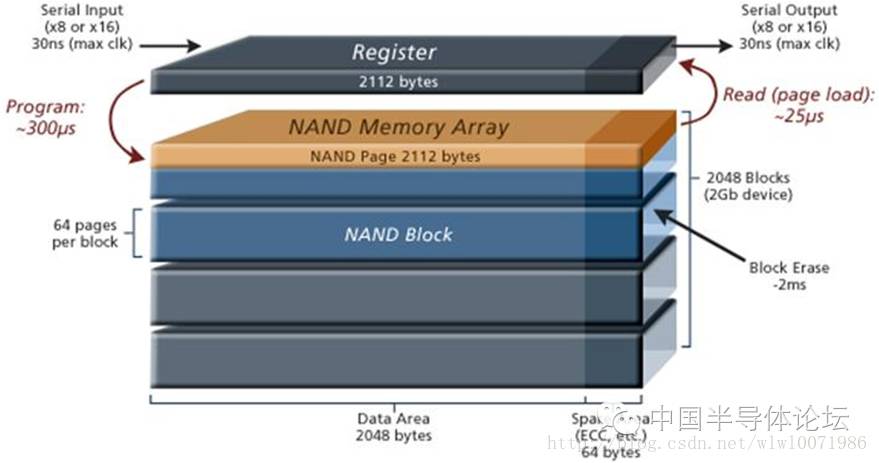
1. The NAND chip is divided into die, plane, block, and page.
2. Chip refers to the packaged chip, which is a single chip.
3. Die refers to the small square on the wafer, and a chip may contain several dies. Due to different flash processes and technologies, the concept of die arises, commonly referred to as Mono Die, a Die, b die, etc. A chip contains N dies.
4. Plane is the smallest unit that NAND can operate on according to read, write, erase commands. A plane is a storage matrix containing several blocks.
5. Block is the smallest erase unit of NAND Flash, and a block contains several pages.
6. Page is the smallest read/write unit of NAND Flash, and a page contains several bytes.
OOB/Spare Area
Each page has a corresponding area called the spare area (Spare Area). In Linux systems, this is generally referred to as OOB (Out of Band).
Data can be easily corrupted during read/write operations, so to ensure data integrity, there must be a corresponding detection and correction mechanism, called ECC/EDC, thus leading to the design of an extra area for storing data verification values.
OOB read/write is completed along with page operations.
The specific uses of OOB include:
► Marking whether the block is a bad block.
► Storing ECC data.
► Storing some file system-related data. For example, jaffs2 uses this space to store specific information, while the yaffs2 file system stores a lot of information related to its file system in OOB.
A 16G NAND storage structure is roughly as follows:
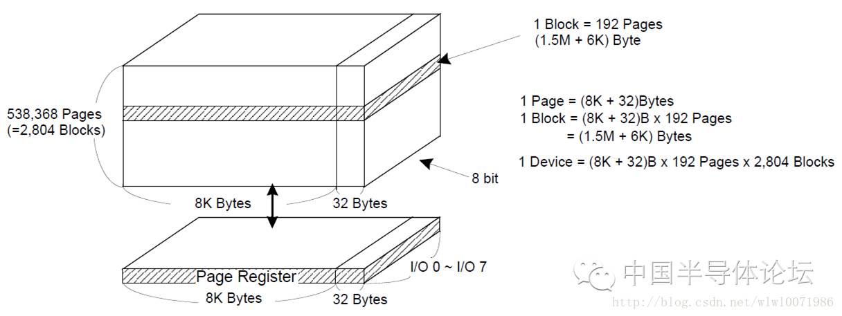
A 16G NAND Flash requires 34 address bits, while the I/O ports for address transmission are 8 bits, so 5 cycles are needed to transmit address information.
Bad Blocks in NAND Flash
A block in NAND Flash that contains one or more bad bits is called a bad block. The stability of a bad block cannot be guaranteed, meaning that it cannot ensure that the data you write is correct, or even if it is written correctly, it may not be read correctly. In contrast, a normal block is guaranteed to write and read correctly.
There are two types of bad blocks:
(1) Bad blocks that exist at the factory:
One type is that when you buy a new NAND Flash, it may already contain bad blocks. These factory bad blocks are called factory (masked) bad blocks or initial bad/invalid blocks, and they are marked as bad blocks before leaving the factory.
(2) Bad blocks generated during use:
The second type is generated during use due to prolonged use. When erasing a block, if an error occurs, it indicates that this block is bad, and it must be discovered and marked as a bad block during program execution. The marking location is the same as above. This type of block is called a worn-out bad block.
SLC and MLC Implementation Mechanism
NAND Flash can be classified into SLC and MLC based on the different levels of voltage stored in the internal data storage units, that is, whether a single memory cell stores 1 bit of data or multiple bits.
► SLC (Single Level Cell)
A single storage cell stores only 1 bit, representing 1 or 0.
For NAND Flash, writing 1 involves controlling the External Gate to charge, ensuring that the stored charge exceeds the threshold Vth, indicating 1.
Writing 0 means discharging, reducing the charge to below Vth, indicating 0.
► MLC (Multi Level Cell)
In contrast to SLC, a single storage cell can store multiple bits, such as 2 bits, 4 bits, etc. The implementation mechanism involves controlling the amount of internal charge, dividing it into multiple thresholds to store different data.
A single storage cell that can store 2 bits is referred to as 2^2 = 4 Level Cell.
Source: Super Energy Network
3D NAND Flash, as a new generation storage product, has received significant attention in the industry! However, currently, 3D NAND is exclusively produced by Samsung Electronics. In the past two months, Toshiba has entered the fray, and now Micron has also announced the development of 3D NAND chips and has already sent samples, marking the end of Samsung’s monopoly. Additionally, Intel has increased its investment in 3D Xpoint at its Dalian factory, signaling an imminent battle in the 3D NAND market.
What is 3D NAND Flash?
From news to reviews, we have reported extensively on 3D NAND Flash. First, we need to understand what 3D NAND Flash is.
3D NAND is like a high-rise building compared to 2D NAND, which resembles a single-story house.
Previously, the flash memory we encountered mostly belonged to Planar NAND, also known as 2D NAND, or simply referred to as NAND. 3D Flash, as the name suggests, is three-dimensional stacking. Intel previously used the analogy of building a high-rise to explain 3D NAND; ordinary NAND is like a bungalow, while 3D NAND is a high-rise building, significantly increasing the building area, theoretically allowing for unlimited stacking.
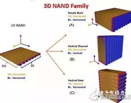
3D NAND vs. 2D NAND
3D NAND Flash is no longer a simple planar memory stack; this is just one structure among others, including vertical channel (VC) and vertical gate (VG).
What are the advantages of 3D NAND Flash?
When answering the advantages of 3D NAND Flash, we first need to understand the issues faced by planar NAND. NAND Flash not only has SLC, MLC, and TLC types but to further increase capacity and reduce costs, the manufacturing process of NAND is continuously evolving from the early 50nm to the current 15/16nm. However, unlike processors, advanced processes, while increasing capacity, also decrease reliability and performance. As the process advances, the oxidation layer of NAND becomes thinner, resulting in reduced reliability, prompting manufacturers to take additional measures to compensate, which in turn increases costs, leading to a point where the process can no longer offer advantages.
In contrast, the approach of 3D NAND to solve problems is different. To increase NAND’s capacity and reduce costs, manufacturers do not need to strive to improve the manufacturing process but can simply stack more layers. This way, the capacity, performance, and reliability of 3D NAND Flash are ensured. For example, Toshiba’s 15nm NAND has a capacity density of 1.28Gb/mm2, while Samsung’s 32-layer stacked 3D NAND can easily reach 1.87Gb/mm2, and the 48-layer version can reach 2.8Gb/mm2.
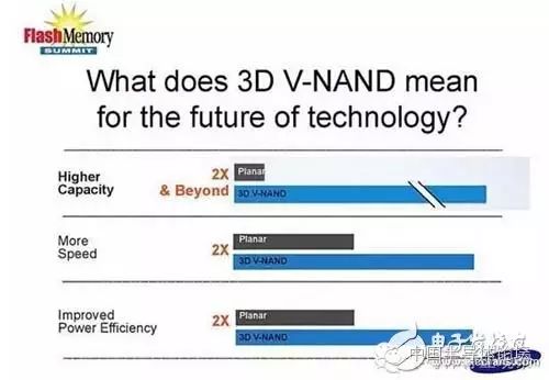
3D NAND Flash has advantages in capacity, speed, energy efficiency, and reliability
Traditional planar NAND Flash is not yet at its end, as the mainstream process is 15/16nm, but the 10/9nm node may very well be the last opportunity for planar NAND. Meanwhile, 3D NAND Flash will continue to thrive, with the current stack layers only at 32-48 layers, and manufacturers are researching 64 layers or even higher stack technologies.
3D NAND Flash and its features from the four major NAND manufacturers
Among the major NAND manufacturers, Samsung was the first to mass-produce 3D NAND, while other companies lag behind by at least two years. Intel and Micron only launched their 3D NAND Flash last year, and Intel just released its first 3D NAND SSD aimed at the enterprise market earlier this month.
The technologies used in the 3D NAND Flash from these four major manufacturers differ, with varying stack layers. In addition to conventional 3D NAND Flash, Intel has also developed a new type of 3D XPoint Flash, which is significantly different from current 3D Flash and is a product worth paying attention to.
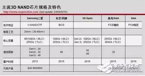
Specifications and features of 3D NAND Flash from the four major manufacturers
Due to manufacturers not necessarily disclosing many technical details, especially rarely mentioning specific manufacturing processes, other manufacturers’ 3D NAND Flash has only just begun to hit the market, with insufficient representative products.
Samsung: The first to mass-produce V-NAND Flash
Samsung is the strongest player in the NAND Flash market and has consistently led in 3D NAND Flash. They began mass production of 3D NAND Flash as early as 2013. In the 3D NAND route, Samsung has explored various solutions, ultimately mass-producing V-NAND Flash with a VG vertical gate structure. They have now developed three generations of V-NAND technology, increasing the stack layers from 24 to 48 layers, with TLC type 3D NAND core capacity reaching 256Gb, used in their 840, 850, and 950 series SSDs.
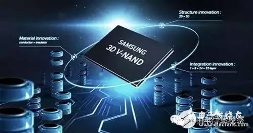
Samsung was the first to mass-produce 3D NAND Flash
It is worth mentioning that Samsung’s lead in 3D NAND Flash is not only due to technological and financial advantages but also because they chose the charge trap flash (CTF) route over the traditional floating gate (FG) technology, which is relatively easier, helping Samsung gain a time advantage.
For detailed technical information on V-NAND Flash, please refer to the previous article: The New Era of NAND, Detailed Explanation of Samsung’s V-NAND Technology.
Toshiba/Sandisk: Unique BiCS Technology
Toshiba is the inventor of flash memory technology. Although their market share and production capacity have been surpassed by Samsung, Toshiba remains very strong in NAND and technology. They have invested in 3D NAND research early on, and in 2007, they uniquely launched the BiCS technology for 3D NAND. As mentioned earlier, 2D NAND Flash can be made into 3D NAND through simple stacking, but the manufacturing process is complex and demanding. Toshiba’s BiCS Flash (Bit Cost Scaling) emphasizes reducing costs with the scale of NAND, claiming to have the lowest core area among all 3D NAND Flash, which also means lower costs.
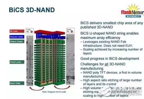
Toshiba’s BiCS technology 3D NAND
Toshiba and Sandisk are strategic partners, sharing technology in the NAND field. Their BiCS Flash began mass production last year, with the current stack layers at 48 layers, core capacity of 128Gb for MLC type, and 256Gb for TLC type, expected to be mass-produced in their Fab 2 factory in Yokkaichi, Japan, with large shipments in 2016.
SK Hynix: The Low-Key 3D NAND
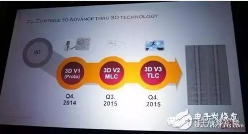
Among these NAND manufacturers, SK Hynix’s 3D NAND is the most low-key, with very few related reports, making it hard to find much information on SK Hynix’s 3D NAND Flash. However, from the information published on their official website, SK Hynix’s 3D NAND Flash has already developed three generations, with the first generation launched in Q4 2014, the second generation in Q3 2015, and the third generation launched in Q4 last year, mainly targeting the mobile market with eMCC 5.0/5.1 and UFS 2.0. This year, the fourth generation 3D NAND Flash will target UFS 2.1, SATA, and PCI-E product markets.
SK Hynix’s 3D NAND Flash stack layers started at 36 layers, but the mass-produced version is 48-layer stack 3D NAND Flash, with core capacity of 128Gb for MLC type and 256Gb for TLC type.
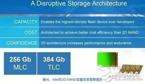
Intel/Micron: The Highest Capacity 3D NAND Flash
Among these manufacturers, Intel and Micron’s 3D NAND Flash came the latest, officially debuting only last year. However, good things come to those who wait; although they lag behind a bit, IMFT’s 3D NAND has many unique features. Firstly, their 3D NAND was the first to adopt FG floating gate technology for mass production, giving them advantages in cost and capacity, with MLC type flash core capacity reaching 256Gb, while TLC flash can reach 384Gb, making it the highest capacity among TLC type 3D NAND Flash.
384Gb capacity is not the end point; at this year’s ISSCC conference, Micron announced a paper on 3D NAND Flash with a capacity of up to 768Gb. Although it may not be mass-produced in the short term, it has already brought hope.
Intel’s Ace: 3D XPoint Flash
IMFT’s slow progress in 3D NAND Flash has raised Intel’s dissatisfaction. Although both parties appear harmonious on the surface, there seem to be differences between Intel and Micron regarding both 16nm and 3D Flash, the most obvious example being Intel beginning to adopt flash supply from competitors. The recently released 540s series drives, for example, used SK Hynix’s 16nm TLC flash instead of IMFT’s.
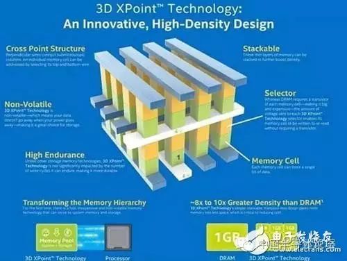 3D XPoint Flash is Intel’s ace for controlling the future of the NAND market
Evidence of Intel and Micron’s discord is also evident—Intel is investing 5.5 billion in upgrading its wafer factory in Dalian, preparing to mass-produce a new generation of flash memory, likely 3D XPoint Flash, which is Intel’s ace.
We have reported extensively on 3D XPoint Flash, which, according to Intel’s official statement, surpasses current memory and flash in all respects, with performance 1000 times that of ordinary memory, reliability also 1000 times that of ordinary flash, and capacity density 10 times that of memory, while being non-volatile, meaning data will not be lost during power outages.
Since it has not yet been released, and Intel is tight-lipped about 3D XPoint Flash, we cannot determine exactly what underpins 3D XPoint Flash. However, a reliable theory suggests it is based on PCM (Phase Change Memory) technology. Intel has been in the storage technology sector for over 20 years, and while its main business is processors, it has never neglected storage technology. It is not impossible that they have achieved a breakthrough in PCM phase change technology.
Compared to current 3D NAND Flash, 3D XPoint Flash could potentially replace both NAND and DRAM memory, as it possesses advantages from both sides. Therefore, in addition to producing various specifications of SSDs, Intel is also preparing to launch DIMM-slot 3D XPoint drives. While it cannot replace DDR memory at present, anything is possible in the future.
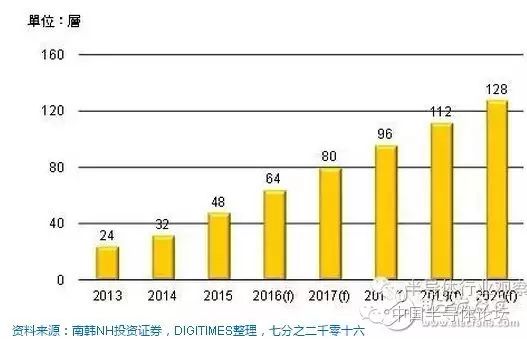
Progress in 3D NAND Technology
In the second half of 2016, in addition to Toshiba (TOSHIBA) starting to sample and ship 64-layer 3D NAND Flash, Samsung Electronics, Micron, SK Hynix, and other memory manufacturers are also set to begin mass production, promoting the vertical stacking of 3D NAND Flash layers from 64 to 80 layers in 2017. According to DIGITIMES research, due to the use of dry etching for 3D NAND Flash with more than 64 layers, the etching speed and accuracy are expected to exceed that of wet etching, increasing the likelihood that Samsung will shift to dry etching for 3D NAND Flash above 64 layers.
Vertical channel 3D NAND Flash refers to the word line (WL) and bit line structure. The vertical channel has cost advantages, making it the mainstream structure for memory manufacturers developing 3D NAND Flash.
As 3D NAND Flash continues to advance towards more than 64 layers, the etching thickness required to penetrate to the bottom will increase compared to before, and the precision of etching will also improve.
The main characteristics of wet etching and dry etching are that wet etching can etch vertically and horizontally simultaneously, while dry etching etches in a single direction. Wet etching can utilize materials that only chemically react with the etched object, providing better selectivity than dry etching.
DIGITIMES research observes that dry etching is relatively suitable for processes with smaller line widths, such as those applied in 3D NAND Flash processes above 64 layers.
Progress of 3D NAND in China
Due to national policies and support from large funds, mainland China is now prioritizing memory chips, and 3D NAND has naturally become a focus for many manufacturers. Wuhan Xinxin Technology (XMC), which was previously acquired by Unisplendour, has already started construction on a 12-inch wafer factory in Wuhan, with the primary goal of NAND flash, directly entering 3D NAND flash. Their 3D NAND technology comes from Spansion, which originated from the merger of the NOR flash departments of AMD and Fujitsu in 1993, and later was acquired by Cypress Semiconductor for $4 billion.
In 2015, Xinxin Technology reached a cooperation agreement with Spansion to jointly develop and produce 3D NAND Flash, mainly based on the latter’s MirrorBit flash technology. However, I searched extensively online and found little information about MirrorBit technology. Both companies’ flash technologies are primarily in the NOR domain, and 3D NAND is evidently lagging behind companies like Samsung, SK Hynix, and Toshiba, with some saying that the stack layers of MirrorBit are only 8 layers. If this is true, it is far behind the mainstream 32-48 layer stacks, and cost advantages are unlikely.
Article recommendations and business cooperation: WeChat ID iccountry