Product reliability is designed.
It is produced and managed.
-Qian Xuesen
1. Circuits Are Designed. Don’t Just Draw, Be a Designer.
An electrolytic capacitor soldered next to a heat sink causes the related circuit parameters to drift, resulting in unstable machine parameters; the inconsistency in the color of green LEDs makes them look unattractive. Each LED has a wavelength requirement, and even if they all emit green light, slight differences in wavelength can lead to color discrepancies, yet the design documents do not specify the wavelength of the LEDs; a certain circuit does not work well, and it is discovered that replacing an inductor on the PCB signal line with a ferrite bead solves the problem, leading to a change in the BOM, and mass production of boards with ferrite beads. Conventionally, it seems that ferrite beads and inductors have similar characteristics, but in fact, ferrite beads exhibit a frequency-dependent resistance characteristic, which is dissipative, while inductors have an energy-storing characteristic. Even if the actual result appears to have no issues after the component change, the true mechanism of the components has not been understood. Although the problem seems to have resolved mysteriously, the hidden virus remains.
There are many similar issues, such as heat dissipation. It seems that thermal design only relates to the temperature within the chassis, ignoring a critical issue: the temperature coefficient. Even if the temperature is not high enough to be scalding, will the increase in temperature lead to drift, and will the parameter values after drift push the component’s characteristic parameters to the edge of normal circuit operation?
For example, derating; almost all engineers say, “We have derated, basically reduced by 50%, the margin is sufficient, and this issue definitely doesn’t exist.” But when derating, have all the parameters that should be derated been reduced to a safe range? When components of the same function are replaced with different packaging forms or manufacturing processes, can the same derating factor yield the same effect? In specific positions and circuits, is it clear which specific parameter should be derated more?
There are also many issues regarding electromagnetic compatibility, vibration, maintainability, testing, etc. Knowing oneself and knowing the enemy ensures victory in a hundred battles. In practical investigations, it is found that there are too many designs that do not know themselves or the enemy. Not knowing oneself means not knowing what one does not know; not knowing the enemy means not knowing the various parameters, conditions, processes, and characteristics faced by the design, which leads to numerous technical issues.
2. Principles of Electronic Reliability Design
The principles of electronic reliability design include: definitions and evaluation indicators of RAMS, reliability models of electronic devices, influencing factors of system failure rates, reliability indicators of electronic products, determination of working environmental conditions, system design and micro-design, process review and testing, design specifications and technical standards.
What are Qian Xuesen’s levels and advantages? Electronics, mechanics, software, testing, management?
None of these; it is systems methodology and engineering calculation.
When we need to decide on the component selection for a circuit, if there is a basic formula that directly tells us which indicators to focus on, component selection and circuit design will follow standards, naturally enhancing our reliability design.
For example, for a socket cable carrying 10A current, is it better to use two 8A wires in parallel or one 14A cable? With reliability models, the answer can be easily obtained.
When driving an LED, is it better to use a transistor or an operational amplifier?
The reliability design of electronic products needs to pay attention to the following basic accuracy:
1. The product structure and circuit should be as simple as possible.
2. Mature structures and typical circuits should be chosen as much as possible.
3. The structure should be simplified, modularized, and plug-in.
4. If a new circuit is adopted, standardization should be noted.
5. New technologies should pay attention to inheritance.
6. Digital circuits should be used as much as possible.
7. Integrated circuits should be used as much as possible.
8. Logic circuits should be simplified in design.
9. Performance indicators and reliability indicators should be considered comprehensively.
10. Traditional processes and habitual operating methods should be adopted as much as possible.
11. New reliability design technologies should be continuously adopted.
12. Common reliability design technologies in electronic products include derating design of components, redundancy design, thermal design, electromagnetic compatibility design, maintainability design, drift design, fault tolerance design, and failure mitigation design, some of which also include software reliability design.
3. Methods to Improve Circuit Reliability Design
The methods for circuit reliability design include derating design (derating parameters and derating factors), thermal design (thermal design calculations, thermal design testing, thermal component selection), circuit safety design specifications, EMC design, PCB design (layout, grounding, impedance matching, processing technology), usability design (usability factors, user operation analysis, design criteria), and maintainability design (maintainability levels, evaluation content, design methods).
A core idea of circuit reliability design specifications is to monitor the process rather than the results.
For example, in thermal design, the heat dissipation method determined by calculating thermal power density and thermal flow density means you don’t have to worry about insufficient heat dissipation; by selecting fans and heat sinks based on thermal resistance and junction temperature calculations, as long as there is enough margin.
1. Derating Design
Derating design refers to a design technique that operates components under stress conditions lower than their rated values. To improve component reliability and extend product life, it is necessary to consciously reduce the working stress applied to the component (such as electrical, thermal, mechanical stress, etc.). The conditions and values for derating must be comprehensively determined to ensure that the circuit can work reliably while maintaining its required performance. Derating measures vary according to the type of components; for instance, resistor derating reduces the ratio of its operating power to rated power; capacitor derating means operating voltage is lower than the rated voltage; derating of discrete semiconductor devices means power consumption is lower than rated values; contact components must reduce tension, torque, temperature, and other limits related to special applications.
Typically, there is an optimal derating range for electronic components. Within this range, changes in the working stress of the components significantly impact their failure rates, making design easier to implement without incurring excessive costs in weight, volume, or cost. Therefore, appropriate derating levels should be determined based on the specific application of the components. If derating is insufficient, the failure rate of components will be high, failing to meet reliability requirements; conversely, excessive derating will complicate equipment design and incur significant costs in weight, volume, and may lead to unnecessary increases in the number of components, thereby decreasing equipment reliability.
Derating levels are divided into three levels: Level I derating, Level II derating, and Level III derating.
Level I derating is the maximum derating; exceeding it offers limited reliability growth, making design difficult to achieve. Level I derating applies to situations where equipment failure poses serious risks to life safety, may cause significant economic losses, leads to task failures, and cannot be repaired economically after failure.
Level II derating indicates that when components are derated within this range, the reliability of the equipment increases sharply, and design is easier than Level I derating. Level II derating applies to situations where equipment replacement will degrade work levels or incur unreasonable maintenance costs.
Level III derating indicates that when components are derated within this range, the reliability growth benefits are maximized, and the design implementation difficulties are minimized. It applies to situations where equipment failure has a minor impact on task completion, does not jeopardize task completion, or can be quickly repaired.
2. Thermal Design
Due to the increasing density of electronic components used in modern electronic devices, thermal coupling occurs through conduction, radiation, and convection among components. Therefore, thermal stress has become a significant factor affecting the failure rate of electronic components. For certain circuits, reliability almost entirely depends on the thermal environment. Thus, to achieve the desired reliability goals, the temperature of the components must be lowered to the lowest achievable level. Data shows that for every 10°C increase in ambient temperature, the lifespan of components is reduced by about half. This is known as the “10°C rule.” Thermal design includes heat dissipation, adding heat sinks, and refrigeration techniques; this paper mainly discusses heat dissipation technology. Common methods include:
The first method is conduction heat dissipation, which can use materials with high thermal conductivity to manufacture heat transfer components or minimize contact thermal resistance and shorten the heat transfer path as much as possible.
The second method is convection heat dissipation, which includes natural convection and forced convection. For natural convection, the following points should be noted:
When designing printed circuit boards and components, excess space must be reserved;
When arranging components, attention should be paid to the reasonable distribution of the temperature field;
Fully utilize the chimney effect;
Increase the contact area with the convective medium.
Forced convection can use fans (like those in computers) or a push-pull method with heat exchangers.
The third method utilizes thermal radiation characteristics, such as increasing the roughness of the heating element’s surface, increasing the temperature difference around the radiating body, or increasing the surface area of the radiating body.
In thermal design, the most commonly used method is to add heat sinks, aiming to control the temperature of semiconductors, especially the junction temperature Tj, to keep it below the maximum junction temperature TjMAX of the semiconductor devices, thus improving the reliability of semiconductor devices. The equivalent thermal circuit diagram of semiconductor devices and heat sinks is shown in Figure 2. The meanings of various parameters in the diagram are as follows:
RTj—thermal resistance inside the semiconductor device, °C/W;
Tj—junction temperature of the semiconductor device, °C;
Tc—case temperature of the semiconductor device, °C;
Tf—heat sink temperature, °C;
Ta—ambient temperature, °C;
Pc—power consumption of the semiconductor device, W.
According to Figure 2, the thermal resistance RTf of the heat sink should be:
RTf=(RTj-Ta)/Pc-RTj-RTc
The thermal resistance RTf of the heat sink is the main basis for selecting a heat sink. Tj and RTj are provided by the semiconductor device, Pc is a design requirement, and RTc can be found in thermal design textbooks. Below is an introduction to heat sink selection.
(1) Selection of Natural Cooling Heat Sinks
First, calculate the total thermal resistance RT and the thermal resistance RTf of the heat sink as follows:
RT=(Tjmax-Ta)/Pc
RTf=RT-RTj-RT.
After calculating RT and RTf, select the heat sink based on RTf and Pc. During selection, refer to the RTf and Pc curves, find the known Pc on the horizontal axis, and then find the corresponding thermal resistance R’Tf of the heat sink.
Select a reasonable heat sink according to the principle R’Tf≤RTf.
(2) Selection of Forced Air Cooling Heat Sinks
When selecting forced air cooling heat sinks, choose suitable heat sinks and wind speeds based on the thermal resistance RTf and wind speed υ.
3. Redundancy Design
Redundancy design uses one or more identical units (systems) in parallel; when one fails, the other units can keep the system operating normally. Redundancy can be classified into thermal redundant reserves and cold redundant reserves; by redundancy level, it can be double redundancy, triple redundancy, or multiple redundancy; by redundancy range, it can be component redundancy, part redundancy, subsystem redundancy, and system redundancy. This design technique is typically applied in critical situations where safety and economic requirements are high, such as boiler control systems, program-controlled switching systems, and spacecraft control systems.
4. Electromagnetic Compatibility Design
Electromagnetic compatibility design is also known as environmental resistance design. First, it is essential to understand what electromagnetic compatibility issues are. Electromagnetic compatibility issues can be divided into two categories: one is when electronic circuits, devices, or systems fail to meet expected technical specifications due to mutual interference or external interference during operation; the other is when devices do not directly suffer from interference but fail to meet national electromagnetic compatibility standards, such as computer equipment exceeding the electromagnetic emission limits or failing to meet requirements for electromagnetic sensitivity and electrostatic sensitivity. To achieve electromagnetic compatibility for devices or systems, techniques such as printed circuit board design, shielding enclosures, power line filtering, signal line filtering, grounding, and cable design are commonly employed. When designing printed circuit boards, the following points should be noted:
Connections at all levels should be as short as possible to minimize parasitic coupling, especially for high-frequency circuits;
High-frequency lines should avoid parallel arrangements to reduce parasitic coupling and should not be bundled like low-frequency circuits;
Design each level of circuits in the order of the schematic to avoid cross-arrangements;
Components at each level should be as close as possible to the transistors and tubes of that level, not distributed too far apart, and should ideally form a loop;
All levels should use single-point grounding or nearby grounding to prevent ground current loops from causing interference. The ground lines for large current and small current should be separated to prevent strong coupling interference from large currents flowing into the common ground;
Elements that generate strong electromagnetic fields and those sensitive to electromagnetic fields should be arranged perpendicularly, distanced, or shielded to prevent and reduce mutual coupling;
Ground lines in strong magnetic fields should not form closed loops to avoid ground loop currents causing interference;
Power supply lines should be close to (the ground of) the power supply and arranged in parallel to enhance power supply filtering effectiveness.
5. Drift Design Technology
Drift is primarily caused by the tolerances between the standard values of component parameters and actual values, environmental condition changes affecting component performance, or performance degradation due to use in harsh environments.
If the drift of component parameter values exceeds their design parameter range, the device or system will fail to perform its specified functions. Drift design is a method to ensure normal operation of a device by writing characteristic equations based on circuit principles during the design phase, then calculating the drift range of the components based on their distributed parameters to keep the drift results within the design range.
6. Interconnection Reliability Design
As most electronic products have connectors, it is necessary to conduct interconnection reliability design to reduce the failure rate of these connections. Common methods include:
Pay attention to connector selection; printed circuit boards should use large or multilayer boards to reduce connection points;
Minimize pluggable points to increase reliability; important components can use redundancy design;
When two plugs are aligned, one should be fixed while the other is floating to ensure alignment during insertion and removal;
Use mechanical fastening methods;
For frequently plugged components, it is best to design them with single-sided routing;
Connection spaces should be orderly and divided;
Feeding and ground lines should be installed discreetly.
In addition, electronic products may also use maintainability design techniques, software reliability design techniques, mechanical part reliability design techniques, fault safety design techniques, and some new reliability design techniques in their reliability design.
4. Reliability Engineering
Reliability engineering is the engineering technology that fights against failures throughout the product’s life cycle, studying the occurrence and development of product failures, handling after failures, repairs, guarantees, and how to prevent failures until they are eliminated.
 It is a discipline related to design, analysis, and testing that aims to improve the reliability of systems (or products or components) throughout their entire life cycle. System reliability refers to the ability to effectively achieve specified functions within a defined time and under specified conditions (such as usage and maintenance conditions). System reliability depends not only on specified usage conditions but also on design technology. Organized reliability engineering research began in the early 1950s in the United States with the study of electronic device reliability. By the 1960s, reliability technology for electronic devices gradually spread to various industries, including mechanics and construction. Later, branches such as failure physics, reliability testing, and reliability management emerged, providing a solid theoretical foundation for reliability engineering.
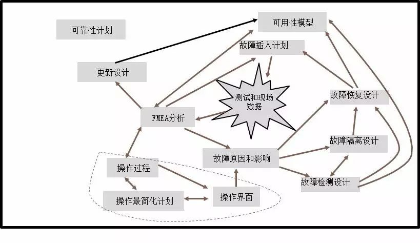
Product reliability is designed, produced, and managed. Reliability engineering encompasses a series of design, management, testing, and production activities aimed at achieving system reliability requirements, related to all reliability activities throughout the product’s life cycle. Reliability engineering is an essential part of product engineering and a powerful tool for achieving product engineering. Utilizing reliability engineering techniques can quickly and accurately identify product weaknesses and suggest improvements and their impacts on system reliability. Reliability engineering is specifically illustrated in the figure below.
During the demand analysis phase, design phase, engineering development phase, and production phase of a product, certain reliability design analyses, management, and testing must be conducted.
According to the product’s hierarchical structure, corresponding reliability work content exists at the system level, device level, component level, and part level, each with unique reliability influencing factors and weaknesses that need to be addressed with appropriate reliability design, management, and testing projects. System designers and project managers need to grasp the development and implementation of reliability engineering from an engineering perspective. The main factors affecting component reliability include the types and quantities of components, rated working electrical parameters and electrical stresses, rated operating temperatures and environmental temperatures, quality grades and quality assurance levels of components, derating characteristics, and thermal sensitivity characteristics of components; the main factors affecting component reliability include the reliability of components themselves and their mutual influences, with key factors being thermal analysis, electromagnetic compatibility, environmental resistance, signal integrity, potential pathways, and processes; the main factors affecting device reliability include mutual influences between components and their structures, processes, and connections; the main factors affecting system reliability include redundancy design, human factors, and system reliability design.
Establishing a reliability engineering system and implementing reliability engineering is necessary for achieving high product reliability. Reliability design analysis is the foundation of reliability engineering; products with poor reliability design levels will inevitably have low reliability. Reliability design requires reliability management, which is the technical management guarantee and organizational structure guarantee for conducting reliability design; the products designed will inevitably introduce “flaws” during the production phase, requiring reliability testing to “expose” them.
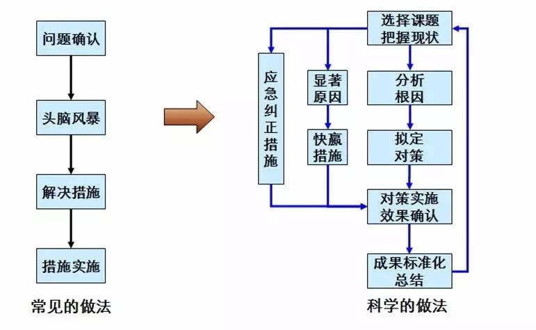
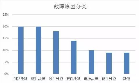 According to statistical analysis of root causes, analyze the main failure causes. Formulate targeted measures for the primary contradictions to achieve rapid reliability improvement.
Reliability engineering integrates reliability testing and design into the design process.
 In the conceptual phase, summarize all reliability requirements; in the planning phase, consider reliability from aspects such as device networking, architecture design, redundancy design, and FMEA design.
During the development phase, implement the planned reliability design; in the verification phase, validate and test reliability requirements.
5. Reliability Testing
From a hardware perspective, reliability testing is divided into two categories:
Reliability testing based on industry or national standards. For example, electromagnetic compatibility tests, climate-related environmental tests, mechanical environmental tests, and safety tests.
Testing projects developed by enterprises based on their product characteristics and quality perceptions. For example, some fault simulation tests, voltage bias tests, rapid power cycling tests, etc.
The following introduces these two types of reliability testing.
1. Reliability testing methods based on industry and national standards
Products will inevitably endure many external stresses during their life cycle. Common stresses include operational loads, temperature, humidity, dust, atmospheric pressure, and mechanical stresses. Various industry and national standards provide the stress levels for specific products under certain application environments, and standard users must select corresponding testing conditions, i.e., stress levels, according to the product’s application environment and quality requirements. This selected stress level essentially becomes the product’s testing specifications.
During the product testing phase, we must apply the corresponding types and levels of stress to a sufficient number of test samples in a laboratory environment to examine the product’s operational stability. For communication devices, common testing items should include at least electromagnetic compatibility tests, safety tests, climate-related environmental tests, and mechanical environmental tests, with many sub-items within these four categories, such as climate-related environmental tests including high-temperature operational tests, low-temperature operational tests, humidity tests, temperature cycling tests, etc. There are many such testing items, which will not be detailed here. Overall, all testing items belong to specification compliance testing (i.e., PASS or FAIL testing), and the purpose of the tests is to simulate the stress types and levels that products will endure during their life cycle and examine their operational stability.
2. Reliability testing methods designed by enterprises
Due to the diverse functionalities of network products and their various application scenarios, the industry and national standards related to reliability testing generally only provide stress conditions for certain types of products, without specifying the operational states or configuration combinations under which the tested devices should be tested. This may lead to the omission of certain test combinations during test design. For example, in frame-based products, the types of line cards, the installation positions of line cards, message types, and system power configurations can all be flexibly combined, resulting in many testing combinations, some of which will inevitably be extreme combinations. For instance, to verify the thermal performance of a frame, the worst testing combination is to fully load the maximum power line card in the frame; when considering the low-temperature operational performance of a line card, the extreme combination is to place the least number of boards with the lowest power consumption in the best cooling position of the frame.
In summary, when designing tests, it is essential to step outside the traditional testing specifications and standards, considering testing design from the perspective of product applications, ensuring that every hardware characteristic and function of the product is fully exposed to various testing stresses under typical application combinations, fully loaded configurations, or extreme testing combinations. Omitting any test combination will inevitably affect product reliability.
The following are two examples illustrating how to design reliability testing methods based on product characteristics.
2.1 Example 1: Parallel Bus Testing for Buffer External Cache of Packet Processors
To cope with burst traffic and manage traffic, network devices typically externalize various random access memory (RAM) to cache packets. Since the packet processing and RAM are interconnected via high-speed parallel buses, the clock frequency of the parallel bus may reach up to 800MHz, with numerous signals and complex topologies. In the context of increasing product device density, products are likely to encounter serious signal quality issues such as crosstalk and switch synchronous noise (SSN). To address these potential issues, careful business design is required to expose the corresponding hardware circuits to adverse physical conditions to see if they operate stably.
Crosstalk, simply put, is a type of interference caused by the routing of signals inside and outside the ASIC. A fluctuation on one signal line can induce unwanted voltage noise interference on other signals. To improve circuit operating speed and reduce power consumption, signal amplitudes are often low, and even a small signal interference can lead to incorrect recognition of digital 0 or 1 levels, significantly impacting system reliability. In test design, a special business load must be applied to the tested device, causing the tested bus to experience a large number of specific signal transitions, exposing the bus to as much crosstalk as possible, and using an oscilloscope to observe whether the signal quality on the bus is acceptable and whether the business is operating normally. For a 16-bit parallel bus, to extreme the crosstalk effect, the test message should have 15 signal lines (the aggressor) transitioning in the same direction while the remaining signal line (the victim) transitions in the opposite direction, resulting in all 16 lines going through this scenario.
Switch synchronous noise is another undesirable physical phenomenon that may occur with high-speed parallel interfaces of RAM. When the drivers of ICs switch simultaneously, large instantaneous changes in current can create AC voltage drops across inductances in the return paths, resulting in noise (referred to as SSN), which may affect the signal level decisions at the receiving end. This represents a very adverse working condition for parallel buses and poses severe challenges to the signal driver’s high-speed signal transition capabilities, driving capabilities, power supply dynamic responses, and power supply filtering design. To verify whether the product operates reliably under such working conditions, a special test load must be applied to the DUT with a specific test message.
For example:
If the tested bus is 16 bits wide, to synchronize the transition of all 16 signal lines, the message content should be:
FFFF0000FFFF0000
If the tested bus is 32 bits wide, to synchronize the transition of all 32 signal lines, the test message content should be:
FFFFFFFF00000000FFFFFFFF00000000
If the tested bus is 64 bits wide, to synchronize the transition of all 64 signal lines, the test message content should be:
FFFFFFFFFFFFFFFF0000000000000000FFFFFFFFFFFFFFFF0000000000000000
If the message exists on the DUT’s internal business channel with buses of the above widths, the business test must load the above messages to see if the DUT operates normally under each message while also conducting signal tests to see if the signals are normal.
2.2 Example 2: Thermal Testing
Thermal testing involves using multi-channel thermometers to measure the temperature distribution of key points or components within the product. The test results are inputs for calculating the lifespan of components (such as E-Caps) and predicting product reliability indicators; it is an important reliability activity during product development.
In general, thermal testing aims to verify whether the product’s thermal design meets the specifications of the operational temperature range; it serves as a laboratory benchmark test, meaning that to ensure consistency in test results, strict requirements must be placed on the test environment. For instance, the tested device must operate without heat sources and forced cooling devices within a specified range, and the surface must not be covered with any foreign objects. However, the working environment of many products differs from the above testing conditions:
Some products may be placed on tables or hung on walls during use, and these devices primarily rely on natural cooling. Different installation methods will directly affect the thermal convection of the device, thus impacting the internal temperature distribution of the device. Therefore, when testing such devices, different installation positions must be considered. Passing thermal tests in laboratory conditions while placed on a table does not guarantee that the device will also pass thermal tests when hung on a wall.
Some network devices are commonly used in internet cafes, and it is common for several devices to be stacked together. When conducting thermal tests on similar products, it is essential to consider whether the thermal tests meet requirements under these conditions.
For some frame-based devices, due to the presence of many slots, the airflow design may have certain dead spots. If the tested object is a service board that can be inserted into multiple service card slots, during thermal testing, the tested board must be placed in the slot with the worst cooling performance, while inserting a high-power service board in the adjacent slot, allowing the tested board to work under full load conditions. Thermal tests should be conducted under such service configuration conditions.
For different product forms, the hardware reliability testing items may vary, but the fundamental testing philosophy remains consistent. The basic idea is to thoroughly analyze the potential application environments of the test object, considering all possible operational states, including extreme operational states, and to create various stress conditions in a laboratory environment, altering the device’s operational states to expose every hardware characteristic and function of the product to various extreme stresses. Omitting any test combination will inevitably affect the product’s reliability.

Manuscript of Qian Xuesen, the Father of Chinese Aerospace