

With the applications of cloud computing, big data, and artificial intelligence technologies, relying solely on CPUs can no longer meet the computing power demands across various industries. Scenarios like massive data analysis, machine learning, and edge computing require a diverse computing architecture, necessitating the collaboration of different processor architectures such as GPUs, NPUs, and FPGAs to meet specific algorithmic and dedicated computing needs. Today, I will take you through an in-depth understanding of FPGA technology.
FPGA stands for Field Programmable Gate Array. It is a product that has further developed based on programmable devices such as PLA, PAL, GAL, and CPLD. It serves as a semi-custom circuit in the domain of Application-Specific Integrated Circuits (ASIC), addressing the shortcomings of custom circuits while overcoming the limitations of existing programmable devices with a limited number of gate circuits.
1. Introduction to FPGA
FPGAs are commonly used to implement digital circuit modules, allowing users to reconfigure the internal logic and I/O modules of the FPGA to meet their needs. They also have the characteristics of static reprogrammability and dynamic in-system reconfiguration, enabling hardware functionality to be modified through programming like software. It is no exaggeration to say that an FPGA can perform the functions of any digital device, from simple 74 circuits to high-performance CPUs. An FPGA is like a blank sheet of paper or a pile of building blocks, where engineers can freely design a digital system using traditional schematic input methods or hardware description languages.
2. History of FPGA Development
The development history of FPGAs is illustrated in the following diagram. Compared to PROM, PAL/GAL, and CPLD, FPGAs offer larger scale and higher performance.

Figure 1: History of FPGA Development
The mainstream manufacturers of FPGA chips include Xilinx, Altera, Lattice, and Microsemi, with the first two accounting for a combined market share of 88%. Currently, all mainstream FPGA manufacturers are American companies. Domestic FPGAs have been in development at least 20 years later than those in the U.S., and are still in the growth phase, limited to low-end applications, with no mature applications in the communication market.
In December 2015, Intel acquired Altera for $16.7 billion. Shortly after the acquisition, Altera formulated a product roadmap for integrating Intel processors with FPGAs. The benefit of integrating these two products is that it can provide innovative heterogeneous multi-core architectures to meet the demands of new markets such as artificial intelligence while significantly reducing power consumption.

Figure 2: History of FPGA Applications in Telecommunications
FPGAs have very mature and widespread applications in aerospace, military, and telecommunications fields. For example, in the phase of integrated telecommunication devices, FPGAs are used for network protocol parsing and interface conversion due to their programming flexibility and high performance.
-
In the NFV (Network Function Virtualization) phase, FPGAs achieve a 5-fold performance improvement in network element data planes based on general-purpose servers and hypervisors, while being managed and orchestrated by the general-purpose OpenStack framework.
-
In the cloud era, FPGAs have been offered as basic IaaS resources to provide development and acceleration services in public clouds, with similar services provided by AWS, Huawei, and BAT.
-
As of now, Intel’s Stratix 10 devices have been successfully applied in Microsoft’s real-time artificial intelligence cloud platform, Brainwave.
3. Recent Developments of Two Mainstream FPGA Companies
Xilinx focuses on leading chips and a rich set of acceleration solutions, securing mainstream cloud platform support through an open strategy, establishing its leading position in data centers. Its UltraScale+ series FPGAs lead competitors by more than a year, giving it an advantage in cloud platform competition. Its VU9P devices are widely used in cloud computing platforms of several companies, including AWS, Baidu, Ali, Tencent, and Huawei.
To meet the growing performance demands for FPGA chips in the accelerator field, Xilinx has released the next-generation ACAP chip architecture aimed at data centers and launched the 7nm Everest device. This device is no longer a traditional FPGA; it integrates ARM, DSP, and Math Engine processor arrays, set to be mass-produced in 2019. Compared to VU9P, the AI processing performance supported by Everest is expected to increase by 20 times.
Intel, on the other hand, provides a full-stack solution from hardware to platform to applications, avoiding open hardware and platform design to prevent ecological fragmentation, resulting in significant investment but slow progress.

Figure 3: Xilinx Product Series Diagram

Figure 4: Intel (Taking Stratix Series as an Example) Product Process Era
In the actual application of FPGAs in data center server markets, there are certain technical difficulties, specifically including the following aspects:
-
1. High programming threshold: Hardware description languages are different from software development languages, requiring developers to have a deep understanding of the underlying hardware; thus, talent becomes an important limiting factor for FPGA applications. It is estimated that there are currently over 20,000 people engaged in FPGA development in China.
-
2. High integration difficulty: FPGA development and application require collaboration between hardware and software, including using high-level languages for system modeling, hardware code (circuit) design, hardware code simulation, and debugging of low-level driver software with hardware logic.
-
3. Longer development cycle compared to software: Hardware development is more complex than software development, resulting in longer debugging cycles.
-
4. Difficulty in obtaining independent logic IP.
4. Overall Structure of FPGA
The architecture of FPGA mainly includes Configurable Logic Blocks (CLB), Input Output Blocks (IOB), internal connections, and other embedded units.
CLB is the basic logic unit of FPGA. The actual quantity and characteristics may vary based on the device, but each CLB contains a configurable switch matrix made up of 4 or 6 inputs, several selection circuits (multiplexers, etc.), and flip-flops. The switch matrix offers high flexibility and, when configured, can process combinational logic, shift registers, or RAM.
FPGAs can support many I/O standards, providing an ideal interface bridging for system design. The I/Os in FPGAs are grouped by banks, with each bank supporting different I/O standards independently. The most advanced FPGAs currently offer more than ten I/O banks, providing flexible I/O support.
CLB provides logic performance, while flexible interconnect wiring is responsible for signal transmission between CLB and I/O. There are several types of wiring, ranging from those designed specifically for CLB interconnections (short line resources) to high-speed horizontal and vertical long lines within the device (long line resources), and to global low-skew wiring for clocks and other global signals (global dedicated wiring resources). Generally, design software from manufacturers will hide the interconnect wiring tasks, making it significantly easier for users.
Embedded hard-core units include RAM, DSP, DCM (Digital Clock Management Module), and other specific interface hard cores. The internal structure of FPGA devices is shown in the following diagram.
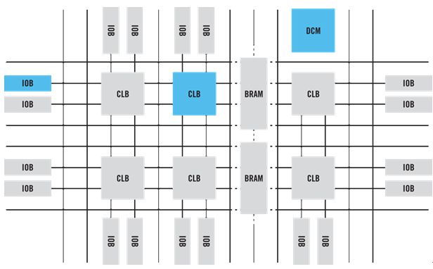
Figure 5: Internal Structure Diagram of FPGA Devices
Generally speaking, the larger the device model number, the larger the scale of logic resources the device can provide. When selecting FPGA devices, users need to refer to this table and consider various needs such as logic resources (CLB), internal BlockRAM, interfaces (number of high-speed Serdes), digital signal processing (number of DSP hard cores), and future expansion to comprehensively determine the most suitable logic device for the project.
5. FPGA Development Process
The design process of FPGA involves using EDA development software and programming tools to develop FPGA chips. The typical FPGA development process is illustrated in the following diagram, including main steps such as function definition/device selection, design input, functional simulation, logic synthesis, layout and routing, and programming debugging.
1. Function definition/device selection: Before starting an FPGA design project, the system function must be defined, and modules need to be divided. Additionally, based on task requirements, such as system functionality and complexity, trade-offs must be made regarding working speed, device resources, costs, and routing feasibility to select suitable design schemes and device types.
2. Design input: Design input refers to the expression of the designed system or circuit using hardware description languages. The most commonly used hardware description language is Verilog HDL.
3. Functional simulation: Functional simulation refers to the logical function verification of the circuit designed by the user before logic synthesis. Before simulation, a testing platform must be built, and test stimuli prepared. The simulation results will generate report files and output signal waveforms, from which the changes in signals at various nodes can be observed. If errors are found, the design must be modified and returned to the logical design. Common simulation tools include ModelSim from Model Tech and VCS from Synopsys.
4. Logic synthesis: Synthesis refers to the process of converting a higher-level abstract description into a lower-level description. Synthesis optimization optimizes the generated logic connections based on objectives and requirements, flattening the hierarchical design for implementation by FPGA layout and routing software. Currently, synthesis optimization refers to compiling the design input into a logic connection netlist composed of basic logic units such as AND gates, OR gates, NOT gates, RAM, and flip-flops, rather than a real gate-level circuit.
A real specific gate-level circuit needs to utilize the layout and routing functionality provided by FPGA manufacturers to generate from the standard gate-level structure netlist produced after synthesis. To convert into a standard gate-level structure netlist, the HDL program must conform to the specific style required by the synthesizer. Common synthesis tools include Synplicity’s Synplify/Synplify Pro software and various synthesis development tools released by FPGA manufacturers.
5. Layout and routing: Layout and routing can be understood as using implementation tools to map logic to the resources of the target device structure, determining the optimal layout for logic, selecting routing channels for connecting logic with input/output functions, and generating corresponding files (such as configuration files and related reports); implementation refers to configuring the logic netlist generated from synthesis onto the specific FPGA chip. Since only FPGA chip manufacturers have the most knowledge about chip structures, layout and routing must choose tools provided by chip developers.
6. Programming debugging: The final step of design is programming debugging. Chip programming refers to generating the data file (bitstream generation) used, loading the programming data into the FPGA chip; afterward, board testing can be conducted. Finally, the FPGA file (such as .bit file) is downloaded from the computer to the FPGA chip on the board.
6. How to Use FPGA
After FPGA development is complete, the final validated loading file is obtained. After outputting the loading file, normal business processing and validation can begin (using software loading methods to describe the entire process).
-
1. Logic loading;
-
2. After the single-board software loads the logic, it needs to reset the logic;
-
3. After the reset is complete, the software must wait for a period until the logic phase-locked loop stabilizes;
-
4. The software starts self-check operations on the logic’s external RAM, internal Block RAM, DDRC, etc.;
-
5. After the software completes self-checks, it initializes all writable RAM spaces and registers of the logic;
-
6. After initialization, the software configures items and registers according to the logic chip manual;
-
7. Once the logic is ready, it can begin processing business.
7. Suitable Scenarios for FPGA
FPGAs are suitable for irregular multi-concurrent, intensive computing, and protocol parsing processing scenarios, such as artificial intelligence, gene sequencing, video encoding, data compression, image processing, network processing, and acceleration across various fields.

“All Store Technical Data Pack (Complete)” e-book, total value 240 yuan (after discount 199 yuan), packed directory as follows (32 volumes):
-
“Analysis, Comparison, and Technical Implementation of RDMA Principles”
-
“Comprehensive Analysis of Data Backup and Replica Management Techniques”
-
“Detailed Explanation of Container Technology Architecture, Network, and Ecology”
-
“Comprehensive Analysis of Flash Memory Technology, Products, and Trends”
-
“The Most Detailed Analysis of Virtualization Technology”
-
“Complete Analysis of Traditional Enterprise Storage Knowledge”
-
“Comprehensive Deep Optimization of IO Knowledge and System Performance”
-
“Complete Analysis of Mainstream Data Center Storage Dual-Active”
-
“Detailed Comparative Analysis of Ceph Technology Architecture, Ecology, and Features”
-
“Detailed Explanation of Data Center Layer 2 Switching Technology”
-
“Detailed Explanation of VMware Cloud Data Center (Private Cloud) Solutions”
-
“Detailed Explanation of Data Deduplication Technology in the Era of Big Data”
-
“Comprehensive Analysis of High Performance Computing (HPC) Technology, Solutions, and Industry”
-
“Summary of Kubernetes Technology and Practice”
-
“Detailed Explanation of DPDK and SPDK Technical Points”
-
“Summary of InfiniBand Architecture and Technical Practice”
-
“Analysis of Mainstream Software, Products, and Vendors in Cloud Computing PaaS”
-
“Detailed Analysis of Cloud Foundry Technology Architecture”
-
“Detailed Explanation of OpenStack Technology and Practice”
-
“Detailed Explanation of SCM/NVM Technology Status and Research Directions”
-
“Detailed Explanation of NVMe Infrastructure and Concepts”
-
“In-Depth Analysis of NVMe Technical Standards and Principles”
-
“In-Depth Analysis of VMware NSX Network Technology”
-
“Complete Analysis of Data Center Server Knowledge”
-
“8 Original Materials from Architect Alliance”
“All Store Technical Data Pack (Complete)” e-book details and content can be obtained through “Read Original“.
Friendly Reminder:
Please scan the QR code to follow the public account, click “Original Link” to obtain the details of “Architect Technical All Store Data Pack Summary (Complete)” e-book data.

