Follow and star our official account for exciting content
Source: Online Materials
Requirement:
In FPGA design, data multiplexers are often required. To achieve parameterized and adjustable designs, we typically need a parameterizable multiplexer, such as M-to-1, where M is an adjustable parameter.
If the multiplexer is non-priority, we can design it using a two-dimensional array in Verilog or VHDL, for example, the synthesis compiler can correctly generate the corresponding circuit.
reg [7:0] din [1:0];assign dout = din[sel];What if we need to design a parameterized multiplexer? How should we design it? Here are three implementation methods:
Method 1: Using Nested if Statements:
Assuming our multiplexer can support up to M inputs in certain cases, we can nest M if statements, thus designing a parameterizable multiplexer with 2 to M inputs.
always@(*)begin if(sel[0])//1 dout = din[0*DATA_SIZE+:DATA_SIZE]; else if(sel[1])//2 dout = din[1*DATA_SIZE+:DATA_SIZE]; else if(sel[2])//3 dout = din[2*DATA_SIZE+:DATA_SIZE]; else if(sel[3])//4 dout = din[3*DATA_SIZE+:DATA_SIZE]; else if(sel[4])//5 dout = din[4*DATA_SIZE+:DATA_SIZE]; else if(sel[5])//6 dout = din[5*DATA_SIZE+:DATA_SIZE]; else if(sel[6])//7 dout = din[6*DATA_SIZE+:DATA_SIZE]; else if(sel[7])//8 dout = din[7*DATA_SIZE+:DATA_SIZE]; else//0 dout = 0;endMethod 2: Using casez:
always @(*)begin casez(sel) 8'b0000_0001 : dout = din[0*DATA_SIZE+:DATA_SIZE]; 8'b0000_001? : dout = din[1*DATA_SIZE+:DATA_SIZE]; 8'b0000_01?? : dout = din[2*DATA_SIZE+:DATA_SIZE]; 8'b0000_1??? : dout = din[3*DATA_SIZE+:DATA_SIZE]; 8'b0001_???? : dout = din[4*DATA_SIZE+:DATA_SIZE]; 8'b001?_???? : dout = din[5*DATA_SIZE+:DATA_SIZE]; 8'b01??_???? : dout = din[6*DATA_SIZE+:DATA_SIZE]; 8'b1???_???? : dout = din[7*DATA_SIZE+:DATA_SIZE]; default : dout = 0; endcase endMethod 3: Using AND/OR Gates:
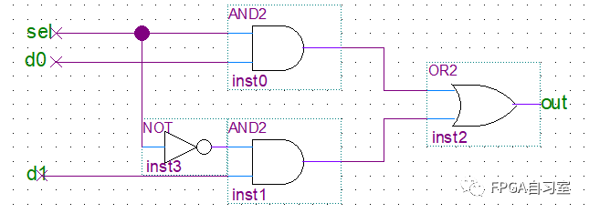
For example, a two-to-one multiplexer should have a structure like this:
A three-to-one circuit structure with priority:
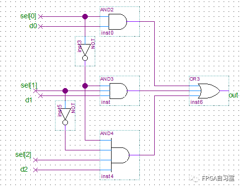
In other words, we can describe such a circuit structure through code and achieve parameterized design through logical replication statements.
The specific idea is to first transform the address signal sel so that only the highest priority bit is 1, while the others are 0. For instance, with low bits having higher priority, sel=1100 changes to sel_prio=0100. Then, sel_prio is combined with the corresponding data, clearly showing that only the data where sel_prio is 1 will be selected, while others will be 0.
module mux#( parameter DATA_SIZE = 8, parameter NUM = 8)( input [NUM*DATA_SIZE-1:0] din, input [NUM-1:0] sel, output [DATA_SIZE-1:0] dout);assign dout = mux_prio(din,sel);function [DATA_SIZE-1:0] mux_prio ; input [NUM*DATA_SIZE-1:0] din; input [NUM-1:0] sel; reg [NUM-1:0] dat; integer i,j; begin for(i=0;i<data_size;i=i+1)begin !temp;="" &&="" (din[i]&&sel[i]);="" ;="" [num-1:0]="" begin="" code="" dat[j]="din[j*DATA_SIZE+i];" din;="" end="" endendfunctionendmodule<="" endendfunctionfunction="" for(i="1;i<NUM;i=i+1)" for(j="0;j<i;j=j+1)" i,j;="" i;="" input="" integer="" mux_prio[i]="mux_prio_bit(dat,sel_prio(sel));" mux_prio_bit="mux_prio_bit" reg="" sel;="" sel[j];="" sel_prio="" sel_prio[0]="sel[0];" sel_prio[i]="sel[i]" temp="temp" temp;="" |=""></data_size;i=i+1)begin>Method 4: Behavioral Description:
In the previous designs, we described the circuit structure of the multiplexer using hardware languages. But can we simply describe its functionality and let the compiler interpret it?
module mux#( parameter DATA_SIZE = 8, parameter NUM = 8)( input [NUM*DATA_SIZE-1:0] din, input [NUM-1:0] sel, output [DATA_SIZE-1:0] dout );assign dout = mux_prio_a(din,sel);// Functional, behavioral descriptionfunction [DATA_SIZE-1:0] mux_prio_a ; input [NUM*DATA_SIZE-1:0] din; input [NUM-1:0] sel; reg temp; integer i; begin temp = 1; mux_prio_a = 0; for(i=0;i<num;i=i+1)begin &&="" code="" end="" endendfunctionendmodule<="" if(temp="" mux_prio_a="din[i*DATA_SIZE+:DATA_SIZE];" sel[i])begin="" temp="0;"></num;i=i+1)begin>Conclusion:
1. This article presents four methods for describing parameterizable priority multiplexers. The first and second methods are conventional descriptions using if-else structures, the third uses HDL based on circuit structure, and the fourth describes functionality using code.
2. The third method appears simpler and easier to understand from a functional description perspective. However, this description method relies on the “intelligence” of the synthesis software because FPGA is based on lookup table (LUT) structure. This description method can be correctly interpreted for simpler circuit functionalities, but is not recommended for more complex circuits.
3. It is crucial to understand the low-level circuit structure in FPGA design. The best implementation process is to go from functionality to circuit to HDL description of that circuit. Using a description similar to the third method is best when one understands the underlying circuit structure and can verify that the synthesized output is the desired circuit.
Reference Blog:https://www.cnblogs.com/wystar/p/7245114.html
📣 IC employment direct camp and chip tape-out course are starting to register!
10+ years of experience in large IC companies, live teaching by IC engineers, focusing on skill improvement and project experience.
Scan the code and reply ‘ZYNQ’ to gain extra black card student status!
👇 Scan the code for details, limited spots available, first come first served 👇