Skip to content
SPI stands for Serial Peripheral Interface, a synchronous serial interface technology introduced by Motorola. It is a <span>high-speed</span>, <span>full-duplex</span>, and <span>synchronous</span> communication bus.
Supports full-duplex communication, simple data transmission rate.
There is no specified flow control and no acknowledgment mechanism to confirm whether data has been received, which leads to certain reliability issues compared to IIC bus protocols.
(1): High-speed, synchronous, full-duplex, non-differential, bus-type (2): Master-slave communication mode.
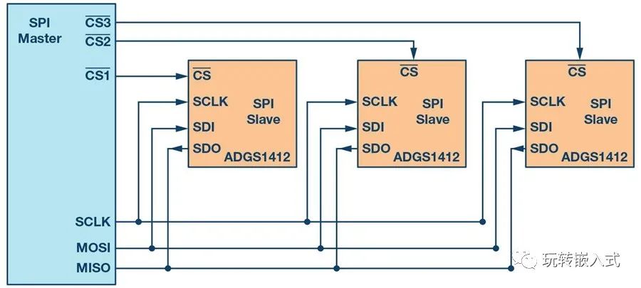
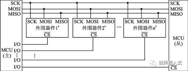
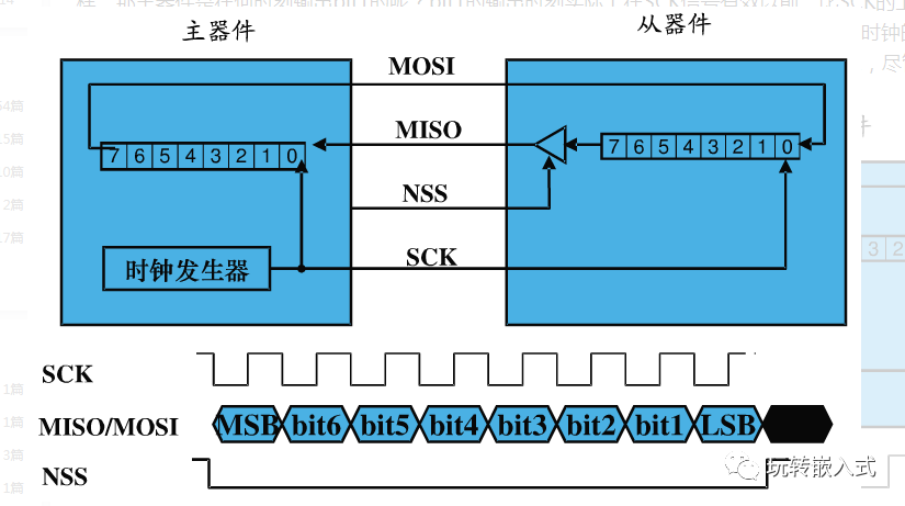
5. SPI Circuit Connection
(1): The communication principle of SPI is very simple. It works in a master-slave mode, usually with one master device and one or more slave devices. There are <span>three-wire</span> and <span>four-wire</span> configurations. The signal lines include <span>SDI</span> (Serial Data Input), <span>SDO</span> (Serial Data Output), SCLK (Clock), and <span>CS</span> (Chip Select).
(2): <span>SDO/MOSI</span> – Master device data output, slave device data input.
(3): <span>SDI/MISO</span> – Master device data input, slave device data output.
(4): <span>SCLK</span> – Clock signal generated by the master device;
(5): <span>CS/SS</span> – Slave device enable signal controlled by the master device. When there are multiple slave devices, each slave device has a chip select pin connected to the master device. When the master device communicates with a specific slave device, it needs to pull the corresponding chip select pin low (generally active low).
6. Analysis of SPI Communication Modes
There are four different modes of SPI communication. Different slave devices are configured with fixed modes at the factory, which cannot be changed. However, both communicating devices must operate in the same mode. Therefore, the SPI mode of the master device can be configured through <span>CPOL</span> (Clock Polarity) and <span>CPHA</span> (Clock Phase).
The specific modes are as follows: Mode0: CPOL=0, CPHA=0; Mode1: CPOL=0, CPHA=1; Mode2: CPOL=1, CPHA=0; Mode3: CPOL=1, CPHA=1.
| Mode |
CPOL |
CPHA |
| Mode0 |
0 |
0 |
| Mode1 |
0 |
1 |
| Mode2 |
1 |
0 |
| Mode3 |
1 |
1 |
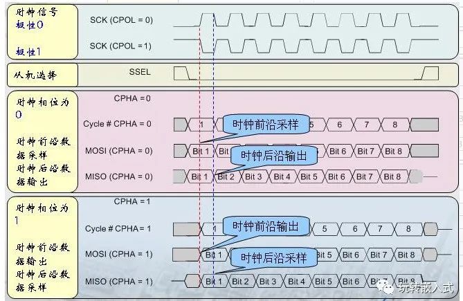
Clock polarity <span>CPOL</span> is used to configure the effective state of the SCLK level; clock phase <span>CPHA</span> is used to configure at which edge the data sampling occurs.
<span>CPOL=0</span> means that when SCLK=0, it is in the idle state, so SCLK is valid when high; <span>CPOL=1</span> means that when SCLK=1, it is in the idle state, so SCLK is valid when low; <span>CPHA=0</span> means that data sampling occurs at the first edge, and data is sent at the second edge; <span>CPHA=1</span> means that data sampling occurs at the second edge, and data is sent at the first edge.
When the SPI master module communicates with the peripheral, the clock phase and polarity of both must remain consistent.
7. Detailed Explanation of SPI Timing
<span>CPOL=0, CPHA=0:</span> In this case, the idle state has SCLK at a low level, and data sampling occurs at the first edge, which is the transition of SCLK from low to high, so data sampling occurs on the rising edge, and data is sent on the falling edge.
<span>CPOL=0, CPHA=1:</span> In this case, the idle state has SCLK at a low level, and data is sent at the first edge, which is the transition of SCLK from low to high, so data sampling occurs on the falling edge, and data is sent on the rising edge.
<span>CPOL=1, CPHA=0:</span> In this case, the idle state has SCLK at a high level, and data sampling occurs at the first edge, which is the transition of SCLK from high to low, so data sampling occurs on the falling edge, and data is sent on the rising edge.
<span>CPOL=1, CPHA=1:</span> In this case, the idle state has SCLK at a high level, and data is sent at the first edge, which is the transition of SCLK from high to low, so data sampling occurs on the rising edge, and data is sent on the falling edge.
Note: The SPI master device can control the clock signal. Unlike UART or IIC communication, SPI communication does not have dedicated communication cycles, start signals, or end signals; thus, the SPI protocol can only control the clock signal line. When there is no data exchange, the clock line must either remain high or low.
For example: Working in mode 0 with this timing (CPOL=0, CPHA=0), as follows:
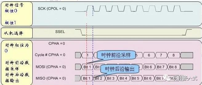
Let’s focus on the first clock cycle of SCK. Data is sampled on the rising edge of the clock (first clock edge), and data is output on the falling edge (second clock edge). First, looking at the master device, the output port (MOSI) outputs the data bit1, which is sampled by the slave device at the rising edge of the clock. When does the master device output bit1? The output time of bit1 actually occurs before the SCK signal becomes effective, half a clock cycle before the rising edge of SCK. The output time of bit1 is unrelated to the SSEL signal. Next, looking at the slave device, the input port MISO of the master device also samples the bit1 output by the slave device at the rising edge of the clock. When does the slave device output bit1? The slave device outputs bit1 immediately after the SSEL signal becomes effective, even though the SCK signal has not yet taken effect.
This diagram clearly shows how the bit1 is output by the master and slave devices.

[1] How to understand clock phase (CPHA) and clock polarity (CPOL) in SPI programming?
[2] Have you ever programmed SPI? What are clock phase and clock polarity?
[3] I2C operation notes – taking AT24C04 as an example
[4] What is the LIN bus? What are the differences between high-speed CAN, fault-tolerant CAN, and LIN bus?
[5] Programming according to timing, driving 74HC595 to achieve seven-segment display
[6] How to statically light up a seven-segment display using a microcontroller?