Source: ICisC Nanjing Integrated Circuit Industry Service Center
With the rapid development of computer technology, microelectronics technology, and network technology, embedded systems have been widely used in various fields such as industry and agriculture. This article mainly provides a detailed introduction to the hardware design of ARM embedded systems and application examples of ARM embedded systems.

ARM Embedded System Hardware Design
Figure 1 is the system hardware structure diagram. The system uses an external 3.6864MHz crystal oscillator to generate the clock required for the core at 18.432MHz, 36.864MHz, 49.152MHz, or 73.728MHz.
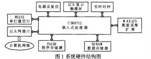
The following mainly introduces the design of the structure, memory expansion, main interfaces, display, and peripherals for this hardware development platform.
1. Power Supply Design
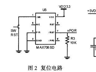
The power supply is essential for the reliable operation of the system, including the power supply and reset circuit. The system reset module provides the CS89712 startup signal. The system uses the nPOR signal as the reset signal, employing a reset chip to generate the reset signal. As shown in Figure 2:
The external power input of the entire system adopts DC 18V-36V. The power supply of the system is relatively complex, with multiple voltage levels. The CS89712 chip I/O and core are powered by 3.3V and 2.5V respectively, while the extended MAX125 and LCD display are powered by 5V. Additionally, the LCD contrast adjustment requires a negative voltage bias (using the MAX686 chip); the operational amplifier power supply voltage used for filtering and voltage following in the MAX125 forward channel is ±12V.
Here, we use Ericsson’s DC/DC power module PKC2131PI, which provides isolated ±12V and +5V. At the same time, we use MICREL’s MIC2211-2.5/3.3BML dual-output LDO to provide 3.3V and 2.5V for the CS89712. Figure 3 shows the dual power supply circuit for the CS89712:
2. Memory Design
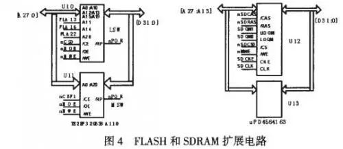
This system uses FLASH to store programs and parameters, and SDRAM as the runtime space for programs, data, and stack. The CS89712 has a built-in SDRAM controller and memory interface. The FLASH part uses two Intel TE28F320B3BA110 chips, forming a 32-bit wide 8MB FLASH, while the SDRAM uses two NEC uPD-4564163G5 chips, forming a 32-bit wide 16MB SDRAM, as shown in Figure 4:
3. LCD Hardware Expansion Design
The liquid crystal display (LCD) has advantages such as rich information display, low power consumption, small size, and light weight, which are unmatched by other displays. It is now widely used in smart instruments and low-power electronic products.
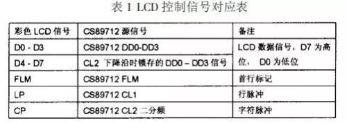
The CS89712 has a built-in LCD controller, which acts like the graphics card of the embedded system. The interface includes the following signals: DD[0:3] (data lines), FRM (frame synchronization signal), CL1 (row synchronization signal), CL2 (pixel data clock), M (AC bias signal). Here, we expand a STN color LCD, which provides an 8-bit data interface. Table 1 shows the corresponding wiring table for the CS89712 and the LCD control signals.
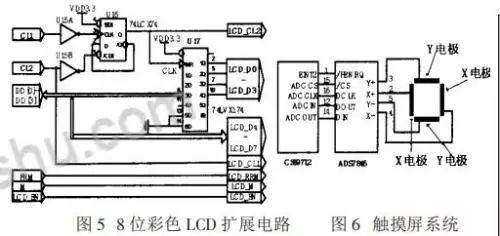
4. Touch Screen Hardware Expansion Design
The touch screen input part consists of the touch screen and the touch screen controller, which, in conjunction with the LCD, can achieve a complete human-computer operation interface. Figure 7 shows the actual touch screen input system part, using a four-wire resistive touch screen. The touch screen controller uses the ADS7846 from T[(BB) Company], which can connect directly to the CS89712 via SPI interface.
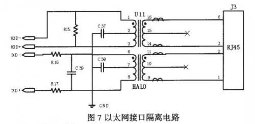
5. Ethernet Interface Design
Since the CS89712 integrates the CS8900A Ethernet controller, which has an 802.3 MAC engine, buffer, serial EEPROM interface, and 10BASE-T analog front end, only an I/O isolation filter and RJ45 interface need to be added. This part of the circuit is shown in Figure 8:
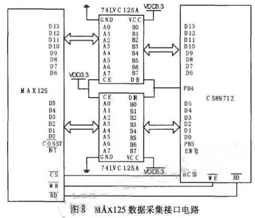
6. Data Acquisition Hardware Expansion Design
MAX125 is a high-speed 2X4 channel synchronous sampling 14-bit successive approximation A/D conversion chip produced by MAXIM, with an analog input range of ±5V. It has a built-in 2.5V reference power supply and includes four sample/hold amplifiers (T/H). The inputs are divided into groups A and B, allowing sampling of eight channels through switch toggling. The converted digital quantities are stored in a 4X14 RAM.
Its parallel interface data access and bus release timing characteristics are compatible with the CS89712 chip bus characteristics, so they can be directly connected without waiting states. Since MAXI25 is powered by +5V, when connecting to the CS89712 with an I/O power supply voltage of 3.3V, a bus level conversion chip 74LVC245A is needed, where the read/write control signal controls the bus conversion direction. After conversion is complete, it automatically requests the CS89712’s external interrupt EINT1, and reading A/D data will automatically cancel that interrupt. By adding limit protection, voltage following, and filtering input circuits in the forward channel, the design of the analog data acquisition circuit can be completed.

Example Application of Tax Control Cash Register
1. Tax Control Cash Register Based on S3C44B0
2. Tax Control Cash Register Composition Block Diagram
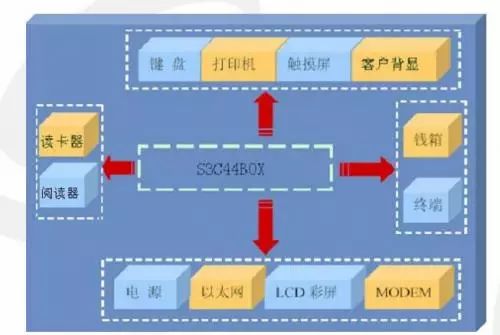
3. Hardware Composition of Tax Control Cash Register
CPU: S3C44B0
Memory: FLASH, SDRAM, NAND FLASH
Display: LCD, VFD
4. POS Machine Software Composition
Operating System
1) Uses uCLinux operating system, no MMU support required, kernel can be trimmed
2) Includes a complete TCP/IP protocol stack, PPP dial-up network
Graphics System
Uses MiniGUI, developed by Chinese developers, with a beautiful interface and easy to port
Application Programs
1) Commercial function modules
2) Tax control function modules
3) Report function modules
4) Management setting function modules
5) Other function modules

Public Account ID: imecas_wx