
In the era of big data, the signal transmission rates of various devices, whether in data center solutions, automotive and industrial equipment, or everyday consumer electronics, are increasing at an unprecedented pace. For example, PCIe 6.0 has reached a transmission rate of 64Gbps; USB4 follows closely with a speed of 40Gbps; and the parallel bus DDR5 has achieved an astonishing rate of 6.4Gbps per second. Meanwhile, the modulation methods for high-speed buses have evolved from traditional NRZ to PAM4, and even higher-order modulation technologies are being explored. Additionally, with the emergence of new bus technologies such as CCIX, GenZ, and CXL, engineers are facing unprecedented challenges.
Improving the success rate and efficiency of PCB design has become a top priority for engineers. Reducing project delays and cost increases caused by rework, and optimizing the design process through high-speed link simulation, has gradually become a focal point in the engineering community. This simulation method not only helps address the aforementioned challenges but also significantly enhances the economic benefits and technical performance of design projects.
The high-speed PCB design process includes the following steps:
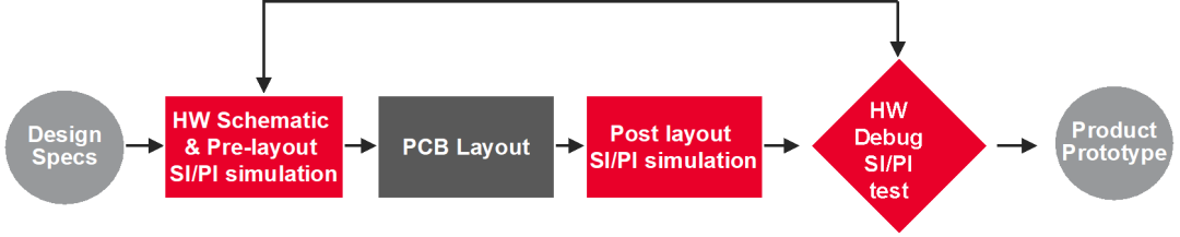
Compared to traditional PCB design, high-speed PCB design requires signal and power integrity analysis during the schematic design phase and after routing is completed. During the prototype testing phase, relevant signal and power integrity tests must be included.
Keysight Technologies’ Advanced Design System (ADS) software is a complete high-speed circuit simulation design platform that provides a comprehensive signal and power integrity simulation solution. Next, we will describe it from the perspectives of schematic design and layout design.
Schematic Design
In the ADS schematic environment, there are three types of simulators that can be used for signal integrity simulation and analysis:
1. S-Parameter Simulator
S-parameters are widely used in both signal integrity and power integrity fields to characterize the properties of various devices, including chip packages, transmission lines, vias, connectors, cables, and passive components such as capacitors. For a complete channel design, multiple S-parameters often need to be cascaded. In ADS (Advanced Design System) software, users can easily implement various S-parameter cascades and flexibly perform S-parameter simulations and data processing.
For individual S-parameters, ADS provides an intuitive S-parameter Viewer, allowing users to easily check S-parameter results in single-ended and mixed-mode. Additionally, this viewer supports the verification of the passivity, reciprocity, and phase relationships of S-parameters and displays Smith charts, providing engineers with a comprehensive data analysis perspective. After completing S-parameter simulations, users can not only view the simulation result curves in the data display window but also further process the data, such as applying specification templates.
Through the application of S-parameter simulations, engineers can analyze key performance indicators such as insertion loss, return loss, and crosstalk in the frequency domain, effectively improving the accuracy and reliability of designs. This method not only simplifies the design process of complex channels but also provides strong support for optimizing product performance.
2. Transient Simulator
Transient simulation is a classic method in time-domain simulation that can analyze various important parameters, including Time Domain Reflectometry (TDR), waveform rise and fall times, ringing phenomena, and eye patterns. During the transient simulation process, the input/output models of chips (such as SPICE or IBIS models) can be combined with channel models for comprehensive simulation. This method allows engineers to comprehensively assess the performance of the entire signal path, optimize designs to ensure signal integrity and system stability, and effectively address potential issues in high-speed circuit design. This simulation approach not only enhances design efficiency but also improves understanding and predictive capabilities regarding complex circuit behaviors.
3. Channel Simulator
For high-speed serial buses, there are typically very strict requirements for Bit Error Rate (BER), with the goal of reducing the BER to a very low level. Therefore, during simulation and testing, a large number of sampling points or specific mathematical algorithms are needed to meet the precise analysis requirements for BER. As signal transmission rates continue to rise, relying solely on the basic driving capabilities of chips is no longer sufficient to overcome the inevitable attenuation of signals during transmission. To address this, chip designs for high-speed serial buses have introduced pre-emphasis and equalization algorithms to improve signal quality.
In the simulation field, this trend has driven the development of new analysis methods, particularly using the Channel Simulation (ChannelSim) tool in ADS. After completing channel simulations, users can view various results, including waveforms, bathtub curves, and eye patterns, in the data display window to comprehensively assess signal integrity. Additionally, IBIS-AMI models or behavioral IO models can be applied in channel simulations to provide more accurate references for designs. To establish IBIS-AMI models, engineers can utilize system simulation software such as SystemVue and ADS provided by Keysight Technologies.
PCB Simulation
1. SIPro/PIPro Simulation Analysis Tools
The layout design environment of ADS integrates the new SIPro and PIPro simulation analysis tools, providing engineers with a fast and efficient method to complete signal integrity (SI) and power integrity (PI) layout analysis and post-layout simulation in PCB design. SIPro and PIPro, as functional modules embedded in the ADS layout design environment, have independent user interfaces and simulation engines, allowing for precise analysis of layout designs.
Furthermore, the ADS layout design environment supports the import of various design file formats, including but not limited to ODB++, Gerber, IFF, EGS, and Allegro Brd, greatly enhancing the flexibility and compatibility of the design process. This integrated solution not only simplifies the management of complex PCB design projects but also facilitates a seamless transition from concept to finished product, ensuring superior electrical performance in designs. By using these advanced tools, engineers can confidently face the increasingly complex challenges of circuit design while improving work efficiency and design quality.
SIPro/PIPro includes the following features:

1. PI-DC for DC Voltage Drop Analysis
Excessive DC voltage drop can cause the voltage supplied to the IC power pins to fall below the recommended minimum operating voltage, leading to IC failure. Additionally, if the current density at vias is too high, it may generate excessive heat, causing damage or burning of the circuit board, resulting in system failure. To address these issues, the PI-DC analysis tool can calculate key parameters such as voltage distribution, current flow, IR Drop (voltage drop), and power loss density in the power distribution network under DC conditions.
With the PIPro tool, engineers can effectively identify the current density at pins and connection vias of chips and other components under DC operating conditions, ensuring the safety and reliability of designs. PIPro can also display the actual voltage at chip pins and provide design margin analysis compared to recommended values, helping engineers assess design risks. Additionally, simulation results can automatically generate detailed reports, facilitating communication and documentation among team members. These features collectively assist engineers in optimizing designs, preventing potential issues, and improving overall product performance and stability.
2. PI-AC for PDN Impedance Analysis
The PI-AC analysis tool is used to evaluate the AC impedance characteristics of the power distribution network (PDN) and can visualize current density to help identify potential hot spots. Through PI-AC, the extracted impedance network can be directly converted into the ADS schematic, allowing for optimization and integration with voltage regulator module (VRM) models and decoupling capacitors. This feature supports the addition of various component models during the simulation process, including but not limited to ideal lumped elements, S-parameter models, manufacturer-provided model libraries, and custom circuit models.
Users can define multiple different models for individual components and easily switch between these models to accommodate different simulation needs. PI-AC analysis also supports the simultaneous analysis of any number of specified power networks, allowing for quick acquisition of new simulation results by simply changing component models without repeating the electromagnetic simulation process. This flexibility and efficiency not only accelerates the design process but also enhances understanding and optimization capabilities for complex power system designs, ensuring that the power distribution network maintains optimal performance under different conditions.
3. PPR (Power Plane Resonance Analysis) for Power Plane Resonance Analysis
Power plane resonance can interfere with sensitive analog circuits and generate excessive electromagnetic radiation, making it difficult for designs to meet electromagnetic compatibility (EMC) standards. Through power plane resonance analysis, the self-resonant frequency of the power distribution network (PDN) and its corresponding Q value can be calculated, providing critical parameter support for designs.
4. Electro-Thermal and Thermal Simulation Analysis for Electro-Thermal Coupled Simulation
In power integrity analysis, electro-thermal simulation functionality has also been integrated to achieve coupled simulation of electrical and thermal effects. This process first conducts detailed simulation of the power distribution network using the power integrity simulation engine (DC Drop) to calculate power density, and then passes this data to the thermal analyzer. The thermal analyzer performs thermal analysis based on the power consumption of the devices, assessing temperature distribution. The system iterates this process multiple times, continuously updating temperature values until the simulation results converge.
5. Power-Aware Signal Integrity Analysis for Power-Related Signal Integrity Analysis
If the reference ground plane is considered while extracting the S-parameters of signal traces without accounting for the power plane, significant errors may occur in the simulation results. To address this issue, SIPro employs a unique hybrid algorithm that can quickly and accurately extract the frequency domain model of signal traces, including vias, between the ground plane and the power plane.
This frequency domain model can be directly converted into the ADS schematic, suitable for various circuit simulation types, such as time-domain transient simulation, channel simulation, DDR bus simulation, etc. This method ensures the accuracy of simulations, allowing designers to identify and resolve potential signal integrity issues early in the design process.
6. CEMI (Conducted EMI) for PCB Power Conduction Simulation Analysis
As EMC testing and analysis are often required in electronic products, conduction is one aspect of EMC. To better discover, avoid, and resolve conduction issues, PIPro can utilize CEMI for conduction simulation analysis of circuits.
7. Fast Impedance Scanning
The simulation speed of SIPro and PIPro has improved by more than 10 times compared to traditional planar or 3D electromagnetic field simulators while maintaining extremely high simulation accuracy, comparable to results obtained using 3D finite element methods. These two tools feature user-friendly interfaces that simplify the simulation process and can easily generate ADS schematics for circuit analysis.
They support simulation of irregular structures and provide convenient back drill via settings, while also allowing users to flexibly define signal, power, and reference terminals. Additionally, SIPro and PIPro are equipped with Python interfaces, making the management of capacitor model libraries more convenient and efficient. After completing simulations, SIPro/PIPro can also generate test benches, facilitating further circuit analysis in ADS schematics.
Overall, SIPro and PIPro provide circuit designers with efficient, precise, and flexible simulation solutions, greatly enhancing design efficiency and flexibility, making them indispensable tools in modern electronic design. These tools not only accelerate product development cycles but also ensure the performance and reliability of the final products.
2. EP-Scan Electrical Performance Scanning Software
SIPro and PIPro are powerful, especially suitable for professional signal integrity analysts. However, during the design phase, hardware engineers, PCB design engineers, and test engineers also need to pay attention to signal and power integrity issues. To assist these engineers in quickly detecting the electrical performance of systems after routing is completed and promptly identifying preliminary SI (Signal Integrity) or PI (Power Integrity) issues, Keysight Technologies has launched the EP-Scan (Electrical Performance Scan) electrical performance scanning software.
With EP-Scan, hardware-related engineers can quickly scan and view the electrical characteristics of signals with simple operations, identifying potential signal integrity issues. This simplicity allows non-professionals to easily get started, effectively improving efficiency and problem discovery speed in the design process. Of course, for more complex signal integrity challenges, the expertise and technology of SI engineers are still required to conduct in-depth analysis and simulation using SIPro and PIPro to resolve these issues.
In summary, EP-Scan provides hardware engineers with a quick and intuitive tool for preliminary assessment and detection of SI and PI issues, while SIPro and PIPro offer strong support for in-depth research and optimization. Together, they promote efficient design and development of electronic products.
EP-Scan can resolve bottleneck issues in signal integrity analysis through three simple steps.
1.
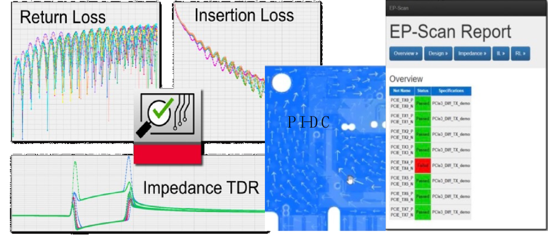
Using EP-Scan, loading PCB layout designs or importing ODB++ files becomes effortless. Next, you can select specific networks for analysis. Even better, you can formulate test plans for the selected networks and choose applicable electrical specifications (EP-Scan includes various standard electrical specifications such as PCIe, USB, DDR, etc.). Based on the selected electrical specifications, detailed analyses of key indicators such as impedance, delay, insertion loss, and return loss can be conducted.
2.
The process of conducting electrical performance scans is very simple; just one click runs all preset test plans. Whenever there are updates to the design, you can automatically rerun the pre-set test plans in EP-Scan to quickly check for signal integrity issues and receive immediate feedback. This method allows for rapid verification of stability and reliability after design modifications, ensuring that each adjustment does not introduce new problems.
3.
After completing the signal integrity analysis, EP-Scan provides a one-click function to generate detailed reports, greatly simplifying the result presentation and archiving process, avoiding tedious manual copy-paste work. Through this function, you can easily share analysis results with team members or management and document the progress and improvements of the design.
Through these three simple steps, EP-Scan provides hardware engineers with a convenient and efficient tool, significantly simplifying the analysis process and saving valuable time and effort. It effectively breaks through the bottlenecks of performance verification, allowing you to focus more on design optimization and improvement, thus accelerating the time to market for products. Utilizing EP-Scan not only improves work efficiency but also accelerates the innovation process, ensuring that your designs meet high standards while quickly responding to market demands.
Test Reports Generated by EP-Scan
In the above content, we briefly discussed the challenges posed by the era of big data on high-speed PCB design and explained how to utilize the two tools, ADS and EP-Scan, to enhance the work efficiency of design engineers. It is worth noting that the advent of the big data era not only raises higher demands for high-speed PCB design but also provides designers with a superior collaborative working environment.
In this context, cloud computing technology is particularly important, especially in engineering fields that require rapid generation of simulation reports. By leveraging the powerful computing resources of cloud computing, the potential of simulation tools can be fully realized. The HPC (High-Performance Computing) acceleration service provided by ADS significantly enhances the speed of engineering calculations, enabling design teams to obtain simulation results in the shortest time, thereby improving project output efficiency.
Moreover, using tools like Cliosoft, design teams can share design files, models, and data in real-time on cloud platforms, supporting collaborative design across multiple locations. This approach greatly accelerates the design process and enhances team collaboration efficiency. In summary, the big data era, by providing advanced computing capabilities and efficient collaboration platforms, not only increases the complexity and requirements of high-speed PCB design but also offers strong support for addressing these issues, driving progress and development across the entire industry.
About Jiesheng Group
Jiesheng Group has expanded and specialized over nearly 20 years from its predecessor, Xiamen Tongchangyuan Electronics Co., Ltd., continuously deepening its focus in the field of instrumentation and equipment, with business scope covering R&D design, manufacturing, trade sales, consulting services, etc. The group is centered in Fujian Province, radiating its business layout nationwide, committed to building a comprehensive group of “trade + factory + finance.” The headquarters is located in Huli District, Xiamen, Fujian, with trade offices distributed in Fuzhou, Ningde, and other locations, and factories located in Xiang’an District, Xiamen; at the same time, offices or companies are set up in cities such as Shenzhen, Shanghai, Beijing, and Xi’an. Among them, the trading company has obtained provincial-level agency rights for several well-known domestic and foreign brands, with products covering electronic testing and material analysis fields.
It independently develops and produces high and low temperature environmental testing equipment, thermal cycling machines, high-end optical microscopes, digital multimeters, and other products. These are mainly applied in the new energy industry, energy storage industry, military industry, aerospace field, semiconductor industry, automotive electronics, intelligent manufacturing, electromechanical industry, and universities.
Since its establishment, the company has adhered to the principles of “integrity, efficiency, and win-win” to provide the best quality services to customers, including technical consulting, pre-sales support, after-sales service, and personalized solutions for industry applications.