In the design of complex systems such as 5G wireless, satellite communication, radar detection, and aerospace control, FPGA engineers play a crucial role.
For an FPGA team, it is essential to complete the product design and verification according to project requirements, ensuring project delivery. To maintain efficient communication and progress among FPGA engineers in increasingly complex system designs, it is necessary to find a suitable design methodology. The goal is to establish a common approach among design teams to enhance the productivity of FPGA design teams while allowing for the exchange of design modules across teams.
Three key factors in FPGA design:
-
FPGA engineering management
-
FPGA design methodology
-
FPGA chip selection
First, it is necessary to establish a predictable roadmap for implementing system design in FPGA. The three steps to achieve predictable outcomes are:
-
Appropriate project planning and scope.
-
Accurately select FPGA chips to ensure that current and future projects can utilize the correct and mature technologies.
-
Follow FPGA design development best practices to shorten design cycles and ensure designs are completed on time, allowing design modules to be reused in future projects at minimal cost.
All three elements need to work smoothly together to ensure successful FPGA design, as shown in Figure 1.
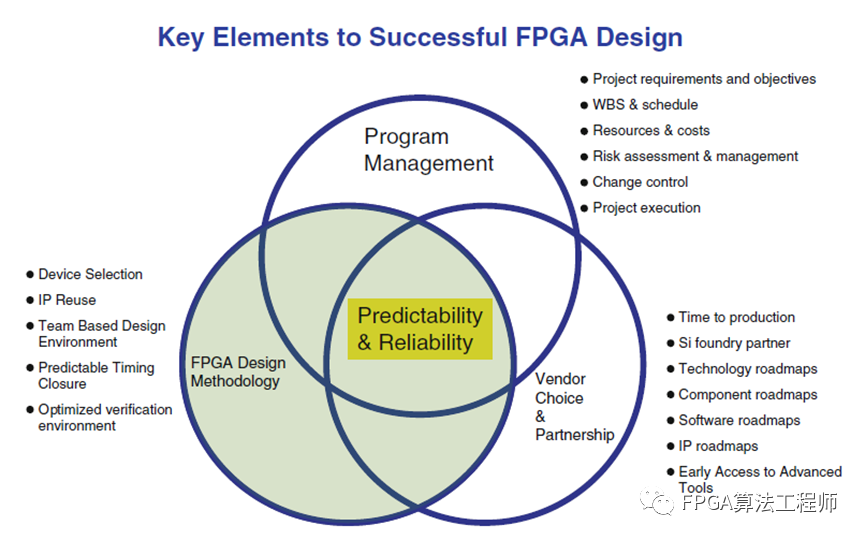
Figure 1 The Three Steps for Successful FPGA Design
The choice of vendor should be a long-term partnership between two companies, especially regarding the licensing of design software and IP Core. By sharing roadmaps and jointly managing existing projects, not only can the success of current projects be ensured, but also the right solutions can be timely provided for future projects. An experience-based tuning process is essential to ensure project success.
FPGA design methodology is the main focus of best practices. This covers the complete FPGA design process from basic to advanced techniques. This approach is independent of FPGA vendors, as it applies to FPGA design practices, but it also needs to be combined with FPGA design software, such as Vivado and Quartus, which have different design environments and related design processes. For FPGA engineers, the design processes are quite similar, allowing for quick transitions. The chart shown in Figure 2 illustrates the best practice design methodology.
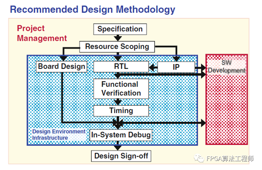
Figure 2 FPGA Design Best Practice Design Methodology
Board Layout, RTL design, IP reuse, functional verification, and timing convergence are often areas where design teams have different design methods, and engineers need to achieve consistent results and shorten design cycles.
Many challenges faced in FPGA design are not unique to FPGA design but are common challenges in design. Compared to ASIC design, FPGA devices themselves do present unique challenges and opportunities. The performance improvements of FPGA devices lead to more complex designs for FPGA, and ASIC engineers can transition to FPGA engineers. This has led many design teams to migrate ASIC design principles to FPGA design. Overall, this benefits the FPGA design process. However, it requires balancing with the benefits brought by FPGA in the design process. The programmable characteristics of FPGA open the door to performing more verification in the system. When used correctly, this can significantly accelerate the verification cycle, but if misused, it can extend the design cycle. The configurable characteristics of I/O present challenges not found in ASIC design. At the same time, the EDA tools used in the industry differ in functionality and cost between FPGA and ASIC.
FPGA engineers need to be familiar with FPGA vendor software, such as Vivado or Quartus design software. FPGA engineers are typically responsible for writing and verifying the design’s RTL code, implementing the design in FPGA, and assisting in the final system integration. FPGA engineers play a vital role in PCB design, responsible for generating FPGA pin outputs from FPGA design software. Therefore, FPGA engineers need to confirm schematics with hardware PCB design engineers, and any modifications require updated pin assignments, ultimately leading to implementation and verification.
In the actual FPGA design process, besides the most basic RTL code design, simulation, and debugging, FPGA engineers also need to be very familiar with the technical routes involved in the project, signal processing processes, system architecture, etc. They often need to participate in the design formulation of system solutions and provide optimal implementation plans.
Thus, for FPGA engineers, the most challenging aspect is not writing RTL code, but rather the involvement in technical solution formulation, architectural design, in-depth understanding of technical protocols, module design and verification, system integration, overall system debugging, and collaboration with other departments within a complex system design.
Additionally, strong leadership is needed to guide the FPGA team, avoiding excessive interference from non-professional leaders in the normal operations of the FPGA team.
During the system design process, various issues often arise, especially during the system debugging phase, where FPGA often becomes the “scapegoat.” FPGA engineers must prove that their designs are sound while also identifying the root causes of issues. The successful launch of each product is backed by a story of “R&D challenges.”
In summary, to achieve complex system design, FPGA engineers need to:
-
Develop detailed design plans and system architectures
-
Master FPGA signal processing and interface design methods
-
Manage engineering effectively and maintain projects
-
Be proficient in the use of instruments and troubleshooting
—END—