By Elite EDA (A learning resource for excellent chip IC layout design, packaging PKG design, and PCB design in WeChat, conveying EDA design information from a professional perspective)
WeChat ID: EDA_Hunter
Follow me to learn more about EDA design technology. For questions or suggestions, please add WeChat (Lavidlee) to contact.

Author: Chen Xi
Mainly sharing learning resources for EDA design, interview skills, workplace phenomena, quickly understanding the EDA design industry, helping those who want to change careers, advance, or grow from beginners to advanced EDA engineers.
If you find this public account helpful, feel free to recommend it to others…


Thank you for taking the time

.

Read this article
In the field of chip design, EDA (Electronic Design Automation) is known as the “mother of chips”. Without it, even the most skilled chip engineers cannot design high-performance semiconductor products.
However, the EDA software market has long been dominated by overseas giants (Synopsys, Cadence, Siemens EDA), with exorbitant prices that have become a significant burden for domestic chip companies. So, how expensive is EDA software? How much do domestic chip companies spend annually on EDA tools? Today, let’s calculate this expense.
1
The exorbitant licensing fees of EDA software
The price of EDA software varies greatly depending on functionality, technology nodes (such as 7nm, 5nm, etc.), and licensing models (buyout or subscription), but overall, the prices are astonishingly high.
The pricing models of the three international giants
Synopsys, Cadence, and Siemens EDA typically adopt a “subscription model”, meaning annual payments rather than a one-time buyout.
High-end tools (for 5nm/3nm chip design): The annual licensing fee for a single tool can reach up toseveral million dollars, and the annual fee for a complete suite can even reachtens of millions of dollars.
Mid-range and low-end tools (for mature processes): Annual fees can range fromhundreds of thousands to millions of dollars.
2. Specific price examples
Digital chip design tools (such as Synopsys’s Fusion Compiler): Annual fee is approximately$500,000 to $2 million.
Analog chip design tools (such as Cadence’s Virtuoso): Annual fee is approximately$300,000 to $1 million.
Verification tools (such as Synopsys’s VCS, Cadence’s Xcelium): Annual fee is approximately$200,000 to $800,000.
Advanced process support (such as 3nm/2nm design kits): Additional charges of30% to 50% apply.
If a chip company wants to cover the entire process from design to verification, its annual EDA software expenditure can reach up to $10 million to $50 million (approximately 70 million to 350 million RMB).
2
How much do domestic chip companies spend on EDA software annually?
The EDA expenditure of domestic chip companies (such as Huawei HiSilicon, Unisoc, Cambricon, etc.) depends onthe company’s size, chip type (digital/analog/AI chips), and process technology and other factors.
1. Large chip companies (annual EDA expenditure in hundreds of millions)
Huawei HiSilicon (before sanctions): Due to involvement in high-end chips (such as the Kirin series), EDA expenditure can reach up tohundreds of millions of dollars per year.
Other leading IC design companies (such as Unisoc, Cambricon): Annual EDA expenditure may range from100 million to 500 million RMB.
2. Small and medium-sized chip companies (annual EDA expenditure in millions to tens of millions)
Mature processes (such as 28nm and above) : Annual EDA fee is approximately5 million to 30 million RMB.
Startups (relying on limited tools): May only need1 million to 5 million RMB, but it is still a significant burden.
This article collects and summarizes information about EDA from the annual reports of 15 listed SoC/MCU/ASIC/edge chip design companies for 2024, aiming to understand their expenditures on EDA tools.
The number of companies disclosing EDA tool expenses in their annual reports is limited, and the disclosed expenses account for a relatively low proportion of overall R&D expenses, approximately 1% level. Generally, annotations are only made when there are significant changes compared to the previous year.However, EDA plays a very important role in chip design, equivalent to the physical education in some regions’ high school entrance exams; although the score proportion is not high, failing physical education directly leads to the inability to apply to certain prestigious schools.Moreover, compared to teachers of other subjects, “physical education teachers” are easier to handle, unlike core subject teachers like “math, language, and English” who have large financial groups and complex forces behind them, making them difficult to manage. Trump managed to handle this well. Several listed chip companies have already warned about EDA risks in their 2024 annual reports—small probability events warned in the financial reports have indeed occurred.1.Rockchip: The long-term payables mention a change ratio of +294.58% compared to the previous period, and “mainly due to the increase in EDA tool purchases this period“.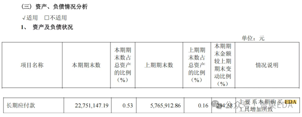 2.Zhongke Lanyun : The accounts payable mention its “EDA tool payment” item, with a “ending balance” of 5,309,734.52 RMB and a “beginning balance” of 6,163,510 RMB.
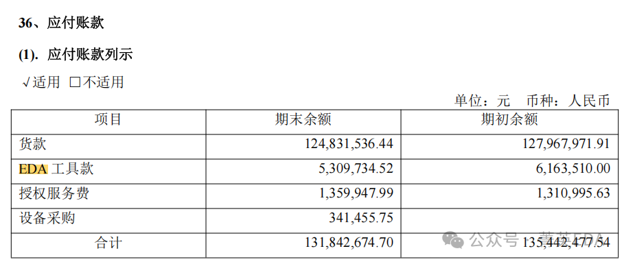 3.GigaDevice : Not mentioned4.Xingchen Technology : Mentioned in operational risks
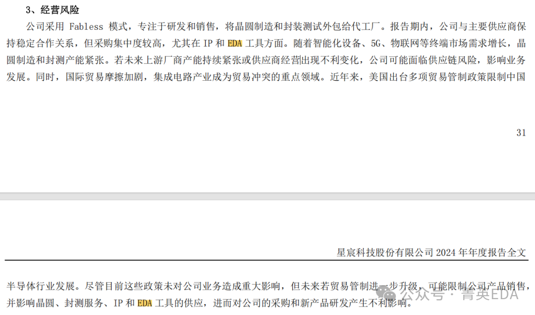 5.Allwinner Technology : Not mentioned6.Puran Semiconductor : “Intangible assets” this period’s ending change +77%, “mainly due to the new purchase of EDA and IP during this reporting period“
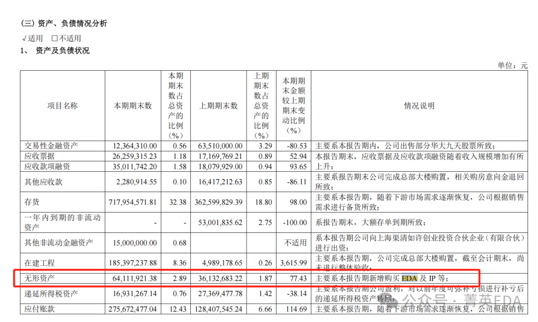 7.Espressif Technology : Not mentioned8.Juchip Technology : Mentioned in “other payables” with a change of +217% compared to the previous period, and “mainly due to the increase in EDA tool payables“
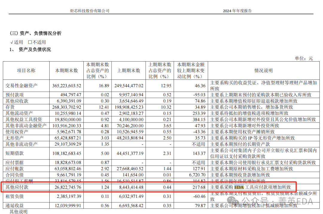 Significant risks are also mentioned.
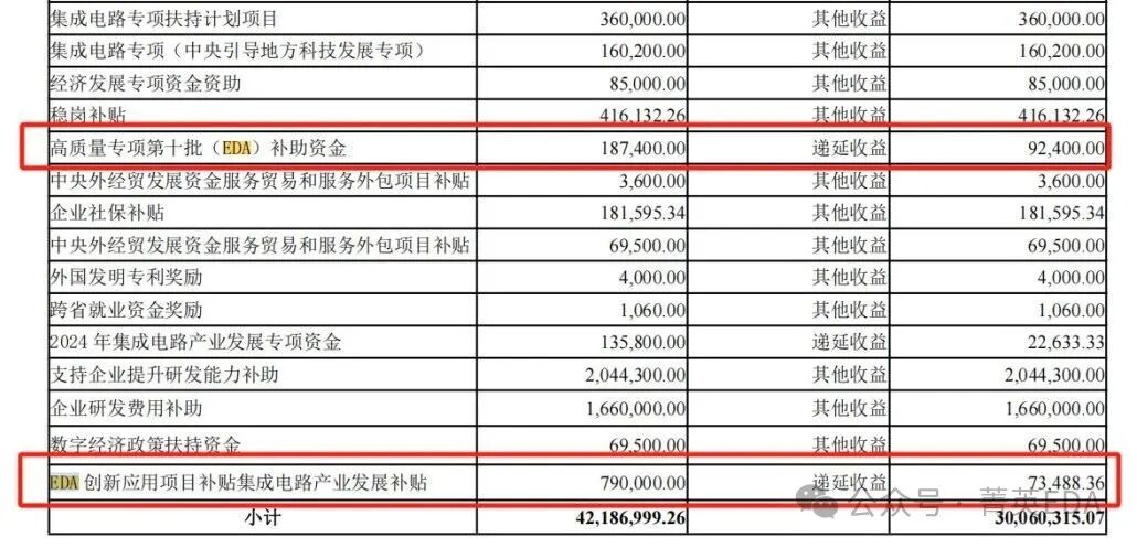
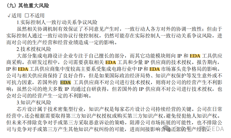 9.Amlogic : EDA innovative applications received government special subsidies
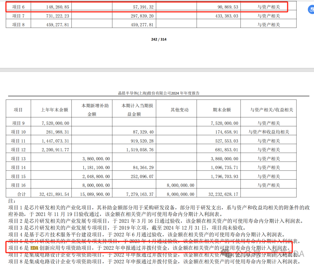 Risks are also mentioned.
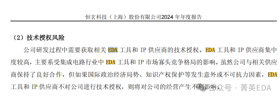 10.Horizon Robotics : Mentioned in risk warnings11.Guokai Technology : This period’s amortization of “EDA tools” in long-term deferred expenses is 370,000 RMB.12.Guoke Micro : Mentioned in risk warnings13.Fuhang Micro : Not submitted14.Beijing Junzheng : Received multiple EDA-related subsidies
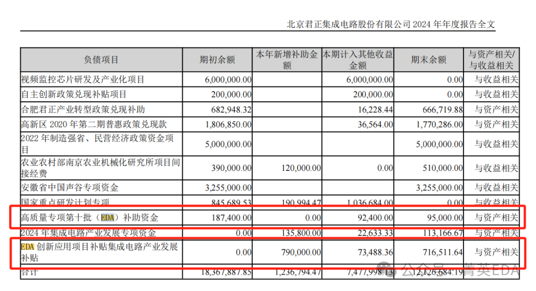
 15.Aojie Technology : Mentioned in risk warnings
3
Why is EDA software so expensive?
EDA software has a long industrial chain, covering all technologies in the entire process of electronic design, simulation, verification, and manufacturing, such as: system design and simulation, circuit design and simulation, printed circuit board (PCB) design and verification, integrated circuit (IC) layout design, verification and testing, digital logic circuit design, analog circuit design, mixed-signal design, embedded system design, co-design of hardware and software, system-on-chip (SoC) design, programmable logic device (PLD) and system-on-programmable-chip (SOPC) design, application-specific integrated circuit (ASIC) and application-specific standard product (ASSP) design technologies, etc. Advanced hardware description languages and IP cores are widely adopted, fundamentally changing the way electronic design and electronic systems are conceptualized.In the field of integrated circuit design and manufacturing, EDA tools exhibit diversity and specialization based on chip types. Integrated circuit chips are mainly divided into two categories: digital ICs and analog ICs.. Digital ICs process discrete digital signals, such as 0 and 1; analog ICs handle continuous signals like light, sound, and temperature. Currently, many ICs are mixed-signal types, combining the characteristics of both analog and digital circuits, usually with the digital part at the core, executing complex algorithms.Depending on the target users and application scenarios, EDA tools can be divided into the following four major categories:Analog design: Used for the design and simulation of analog signal processing circuits. These tools help designers optimize the performance of analog circuits, ensuring their accuracy and reliability when processing continuous signals.
Digital design: Used for the design and verification of digital circuits, including front-end design, front-end verification, back-end design, and back-end verification. These tools are widely used in the development of digital ICs, ensuring their functionality and performance meet expectations.
Wafer manufacturing: Used for design and optimization during the wafer manufacturing process. These tools help manufacturers improve wafer production efficiency and quality, reducing defects and costs.
Packaging: Used for IC packaging design, ensuring the physical protection and electrical connection of chips in the final product. These tools can optimize packaging forms, improving heat dissipation and mechanical strength.
There are reasons for the high cost of EDA software. In1988, the country mobilized 17 units and over 200 experts to Beijing to discuss a major issue, which was to develop its own EDA software system.In 1993, China’s first EDA tool with independent intellectual property rights was born, named “Panda EDA“, symbolizing the preciousness and rarity of EDA. 
At that time, “Panda EDA” lagged behind the three giants by about 5 years, but its price was only 1/10, so some overseas chip manufacturers with lower requirements began to adopt “Panda EDA” software.
Unfortunately, After more than 10 years of hard work, Huada Jiutian has made breakthroughs in four major areas: analog circuit simulation software, digital SoC IC design, dedicated EDA tools for wafer manufacturing, and flat panel display design.Although domestic EDA has achieved significant results, the three international giants still occupy over 85% of the global market share, and in many areas, domestic EDA remains blank, forcing chip companies to purchase software from the three giants, keeping EDA software prices high for several reasons:
1. Technological monopoly
Synopsys, Cadence, and Siemens EDA occupy over80% of the global market share, leaving domestic companies with weak bargaining power.
2. High R&D costs
EDA software requires continuous updates to support the latest processes (such as 3nm, 2nm), leading to huge R&D investments.
3. Bundled sales
EDA giants typically require customers to purchase theentire suite of tools, rather than individual modules, further driving up costs.
4. Additional charges for advanced processes
The more advanced the process, the higher the price of EDA tools, and additional “technical support fees” may be required.
4
EDA is the “invisible tax” of the chip industry
From circuit design to simulation, and then to physical realization, EDA software plays a crucial role in every step of chip design. Without EDA software, chip design would be impossible.
Furthermore, the market monopoly and high costs of EDA software make it an “invisible tax”. The global EDA market is highly concentrated, with Synopsys, Cadence, and Siemens EDA controlling 85% of the global market share, and the Chinese market is firmly dominated by these three companies. This market monopoly leads to high EDA software prices, which is a significant expense for chip design companies.
In addition, technical barriers and the need for upgrades also make EDA software an “invisible tax”. With the advancement of Moore’s Law and continuous improvements in chip processes, EDA software needs constant upgrades to meet new design requirements. This not only requires substantial R&D investment but also necessitates close collaboration with equipment manufacturers, creating high technical barriers and upgrade costs.
For domestic chip companies, EDA software is aninevitable high cost, especially when involving high-end processes, with annual expenditures reaching hundreds of millions of RMB. In the current international environment, accelerating the development of domestic EDA has become a consensus in the industry, but this path remains challenging.
With the recent U.S. ban on domestic EDA, the three major EDA giants have begun to respond. Even if there is money to buy the EDA software from the three giants, it may no longer be feasible. Many companies that have previously purchased EDA software from the three giants can continue to use it, but as the scale of R&D personnel increases, adding new users will no longer be possible.
How many years do you think it will take for domestic EDA to catch up with the three international giants? Feel free to leave comments for discussion!
Interactive benefits: The highest number of likes in the comments will receive a copy of the e-book “Cadence High-Speed Circuit Design – Case Analysis and Implementation Based on Mobile High-End Boards” written by the author
Follow us to unlock more hardcore knowledge about PCB design!Have you encountered difficulties in PCB design? Feel free to share practical cases in the comments!

Previous articles review:
[1] The interviewer asks, “Can you read eye diagrams?” You must answer “I don’t know”: Revealing communication wisdom in technical interviews
[2] The online platform for EDA design learning has been completed, please enter here to watch
[3] Countdown to the first EDA advanced board design class in 2025, only 1 day left
[4] Discussing the four “no” principles for the placement of silkscreen in PCB design[5] How to handle bending areas, reinforcement areas, adhesive areas, easy-to-crack areas, copper-leak areas, silver paste areas, silver mesh areas, and silver film areas in FPC design?[6] What is the “sandwich” stacking structure? Why are mobile phone motherboards keen on the “sandwich” structure?[7] What is gold wire positioning? Why are high-density boards keen on gold wire positioning?[8] Discussing the holes used in HDI advanced PCBs[9] How to perform thermal treatment on individual pads in Cadence design[10] The U.S. 3D991 ban strikes! The entire chain of China’s semiconductor industry faces a bottleneck crisis. This time, we aim not only for replacement but also for surpassing.