Next, let’s look at the differences between RevC and RevB:
1. In RevB, the relative position of resistor R88 and fuse F1 was incorrect. Additionally, the DC choke (power choke) we added can reduce noise, but it connects PGND and GND. There should be no DC potential difference between these two points. However, under certain computers + operating systems, there may be an AC potential difference of 250mV. Since the internal comparator of the Microchip USB3320 chip is referenced to GND, it may cause the chip to switch abnormally between USB host and device modes. A temporary solution is to change the resistor R88 on the back of the USB port from the recommended 1k ohms to 24.9k ohms.
2. We found issues during the ESD electrostatic discharge tests, so we need to add ESD protection on the RF connector.
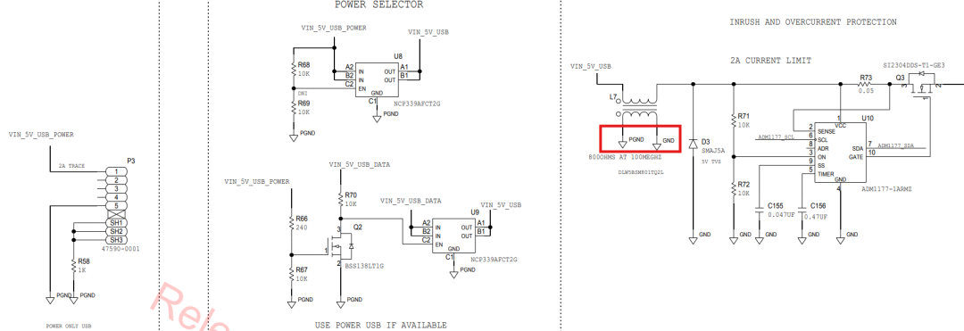
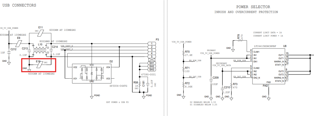
3. We reduced costs in the power design (and made improvements) by replacing the NCP339AFCT2G and the surge and overcurrent protection ADM1177 with LTC4413 (actually used LTC4415 in the schematic). In RevB, the NCP339AFCT2G is designed to disconnect before reconnecting, so if you connect the device to a computer via USB, the device will power on, and if you then provide external power, the device will experience a brief power interruption before recovering. Although this issue is not severe, changing the chip can improve operational continuity. However, after changing the chip, you cannot use ADM1177 to read USB voltage and current.
4. We have introduced another RF channel.
Point 1:
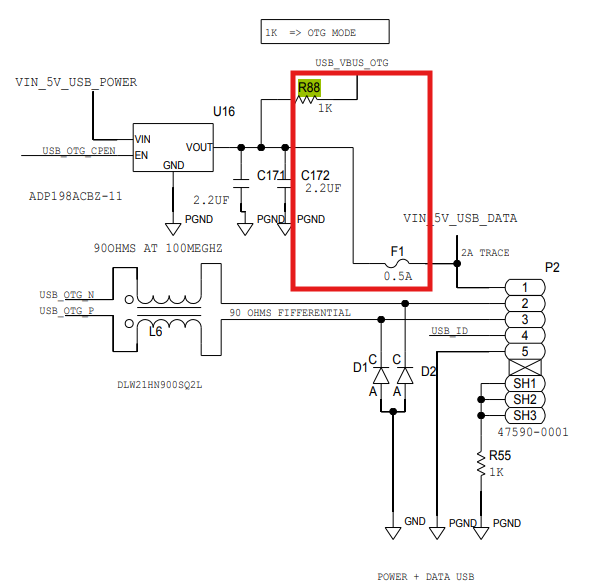
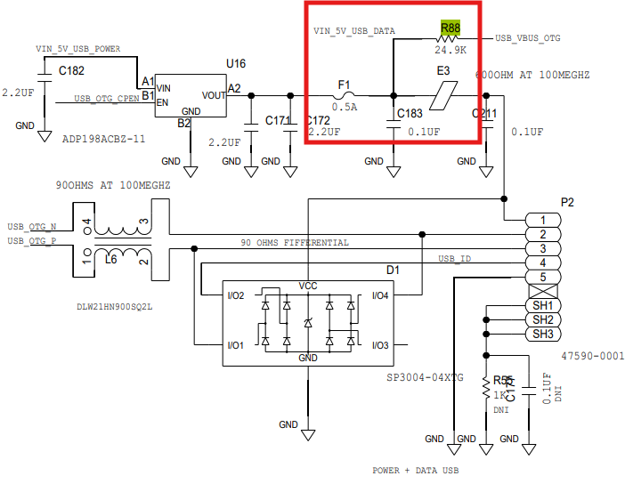
In RevC, the relative positions of R88 and F1 have been changed, as well as the resistance value of R88.
In RevB, the power choke connects PGND and GND on the same side of the inductor, effectively shorting them together at low frequencies, but if there is a potential difference between these two pins, it can cause issues.
In RevC, the bottom of the choke is all GND. Additionally, it can be seen that the USB port, which was originally only used for power, now also utilizes the data line, which connects through a serial conversion chip to ZYNQ PS. This way, the serial debugging port that was previously brought out on RevB can now be replaced by the USB power port, assisting users in debugging.
Point 2:
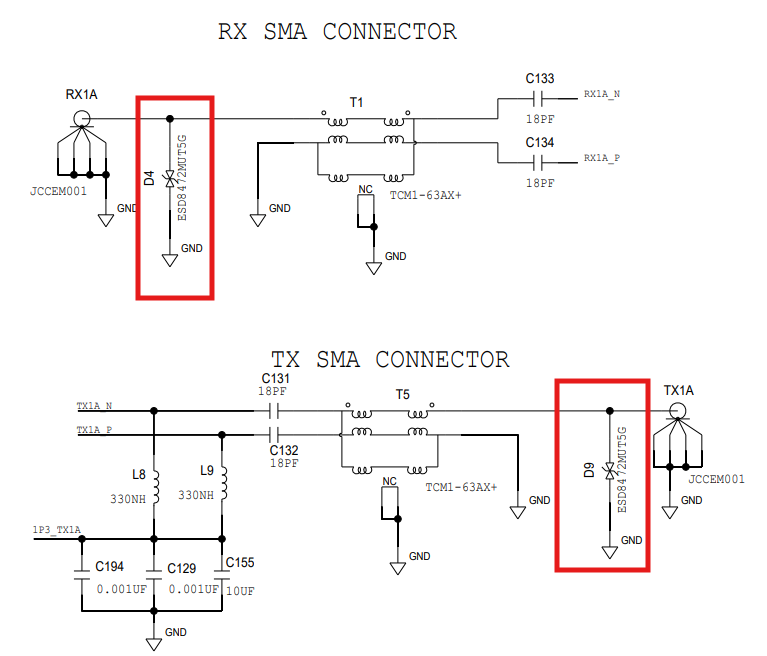
Compared to RevB, in RevC, ESD8472MUT5G bidirectional ESD protection chips have been added near the antenna ports for receiving and transmitting.
Point 3:
In fact, points 2, 3, and 4 in the diagrams reflect that the previously used NCP339AFCT2G and ADM1177 are now replaced with LTC4415. These chips are mainly used for overcurrent protection and surge protection, and the part not captured in the screenshot on the far right is their output, named VIN. This VIN will connect to several buck converter chips, ultimately reducing to various voltages to power multiple power rails.
Point 4:
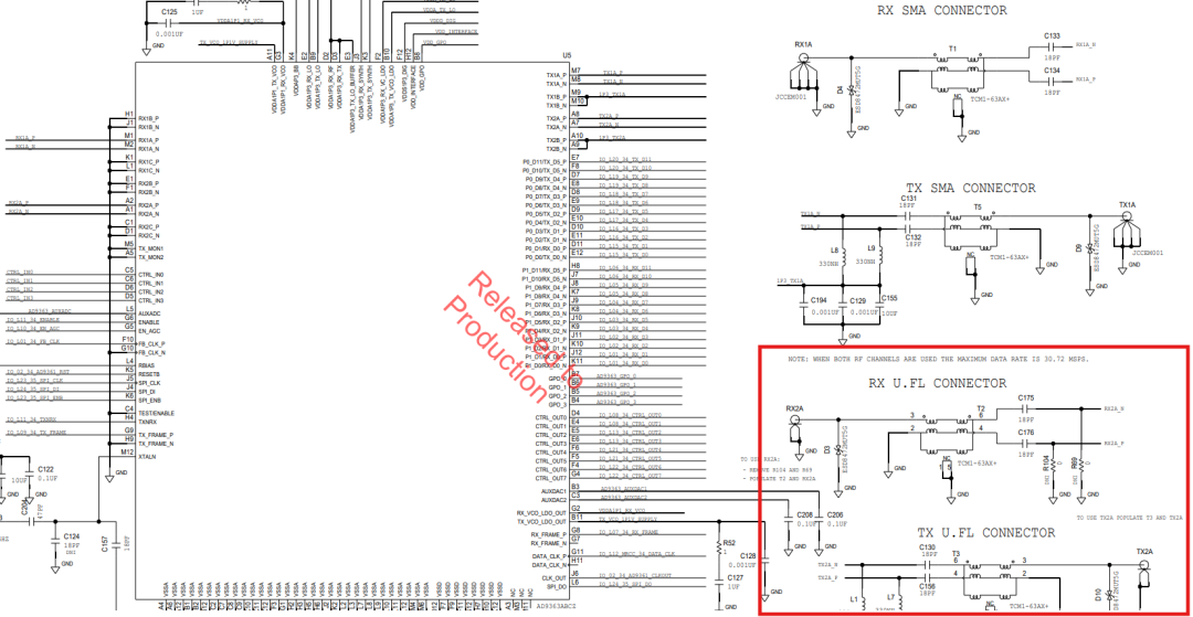
Compared to RevB, in RevC, a second receiving and transmitting channel has been brought out from the AD936x chip, but these two channels are not SMA ports but smaller U.FL ports.
It should be noted that when the RF channels are used more, the sampling rate will decrease.
And one last point:
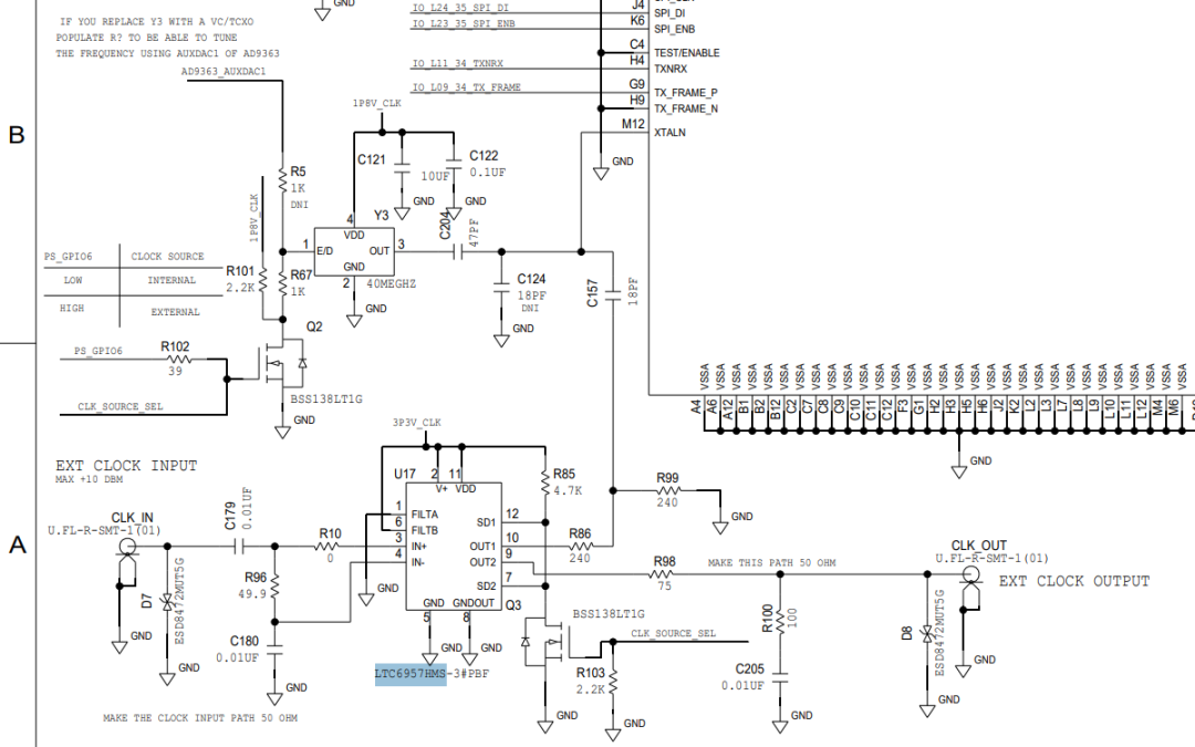
This point is not particularly clear on the official website, but it is also an addition in RevC compared to RevB. In RevB, the enable pin of the 40MHz clock chip is connected to an internal pull-up signal, indicating that this clock chip is always enabled. However, in RevC, you can use PS‘s GPIO6 or CLK_SOURCE_SEL signal to pull it to ground, thus disabling the output of this clock chip. At this point, you can use the LTC6957 chip to provide the signal from CLK_IN connected to the U.FL port to AD936x‘s XTALN, achieving frequency synchronization.
Additionally, the LTC6957 chip can also forward the signal on CLK_IN to CLK_OUT for synchronizing other devices. However, it seems that it does not support outputting the internal signal of the 40MHz crystal oscillator chip to CLK_OUT. This means you need an external clock source for two devices, and cannot use one device’s clock output for another device.