Reference:https://wiki.analog.com/university/tools/pluto/hacking/hardware#schematics
Since its release in2017 until the end of the English documentation in2023, the official version has undergone several revisions (Rev). These areA,B,C,D. However, according to the description,C and D are essentially the same. The hardware version number can be found on the device’s built-in webpage; if you findRevC, it means you are actually usingRevD.
I have roughly looked at it, and the main modifications focus on the power supply section, with some changes made to addressUSB interference issues.
Below are the differences betweenRevB and RevA:
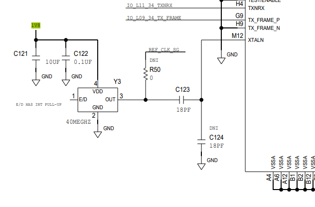
1.RF performance issues (EVM only achieved-32dBm, with a target of-45dBm). The reason is that theRakon RXO3225M 40MHz crystal oscillator’sPPSR (Power Supply Rejection Ratio) is insufficient. InRevA, a1.8V digital power rail (which has more noise) was used to power this crystal oscillator. Attempts were made to useLC filtering or ferrite beads, but ultimately theLDO chipADM7160ACPZN1.8 was used to power the crystal oscillator, which yielded the best results.
2. Even after adding theLDO, RF performance was still inadequate on some computers due to noise from theUSB power supply. After we added theDLW5BSM801TQ2L power choke in series, the performance improved.
3. Power supply noise affects RF performance, so we synchronized multiple switches to reduce input ripple, which also allowed us to decrease the total input capacitance on the device.
4. The device had noise at480MHz, which nearly caused it to fail theFCC test, and this480MHz also interfered with its own RF reception. Therefore, we added theDLW21HN900SQ2L (90 ohm choke) on the USB data line.
5. TheQSPI and DDR3L models were replaced to resolve the issue of the old models being discontinued.
6. Additional test points were added.
7. TheUSB port was enhanced withOTG functionality, and the power supply circuit was modified to monitorVBUS, etc. These changes were initially considered low risk (later found to cause issues, leading to further modifications inRevC).
Point 1:
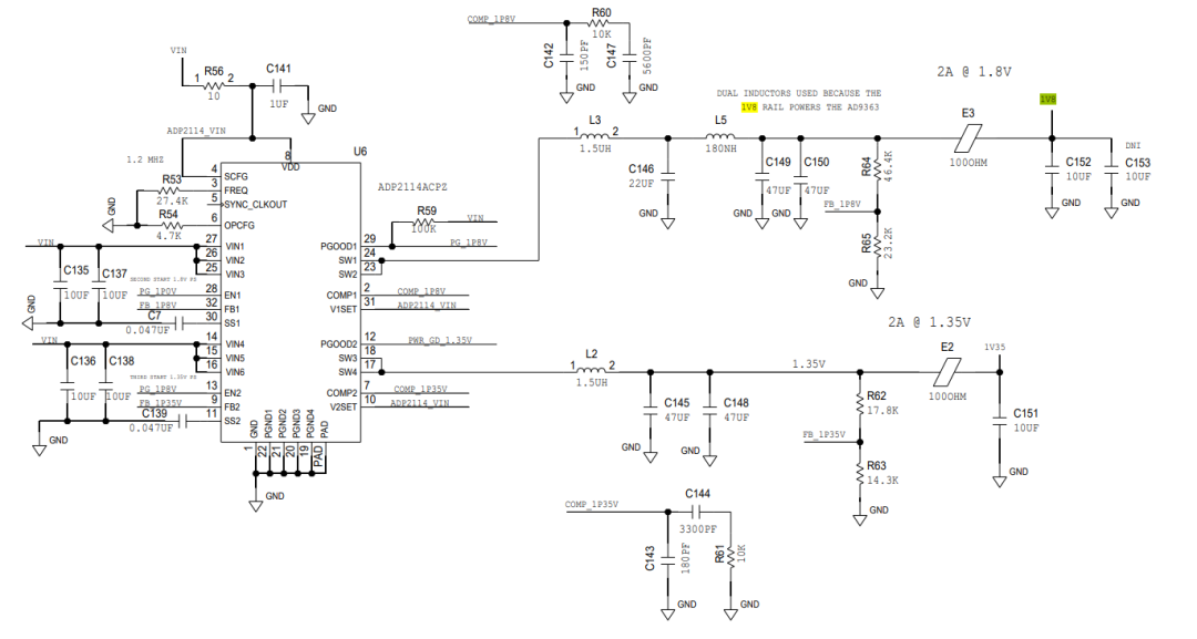
InRevA, theADP2114ACPZ switching power supply chip was used to reduce5V onVIN to1.8V to power various digital chips, while also powering theRakon crystal oscillator.
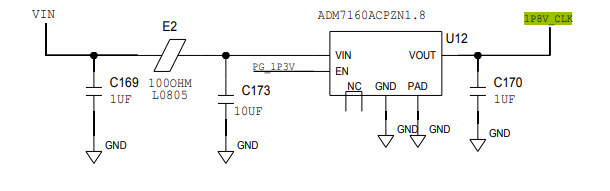
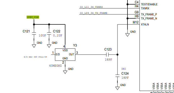
InRevB, theADM7160ACPZN1.8 linear regulator chip was used to reduce5V onVIN to1.8V to only power theRakon crystal oscillator.
Point 2:
Before looking at this point, it is important to understand the roles of the twoUSB ports on this board. One port is purely for power supply, without data transfer. The other port can handle both data and power supply.
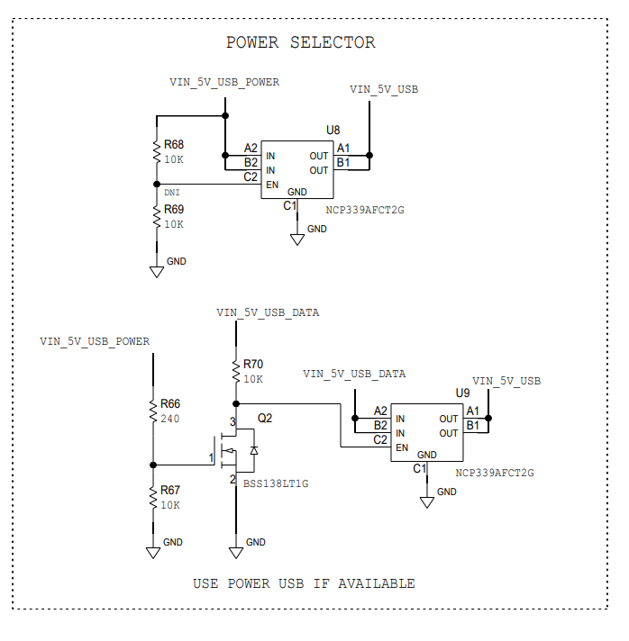
In the schematic, the5V power pin for the former is calledVIN_5V_USB_POWER, while the latter’s5V power pin is calledVIN_5V_USB_DATA. Then, through the schematic’sPower Selector section, one of them is selected asVIN_5V_USB.
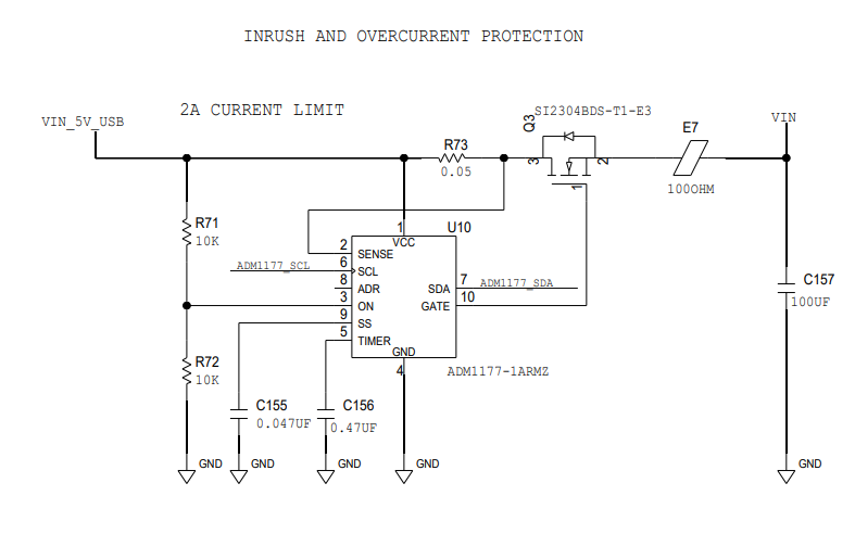
After obtaining thisVIN_5V_USB, it cannot be directly supplied to other circuits. InRevA, it goes through theADM1177 hot-swap controller for surge and overcurrent protection before being used asVIN to supply other chips.
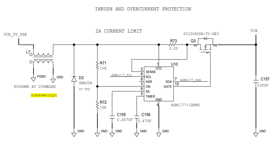
InRevB, aDLW5BSM801TQ2L power choke must be connected in series before the surge protection chip.
Point 3:
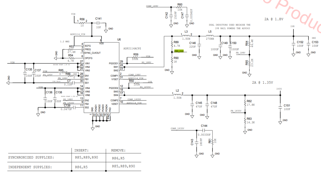
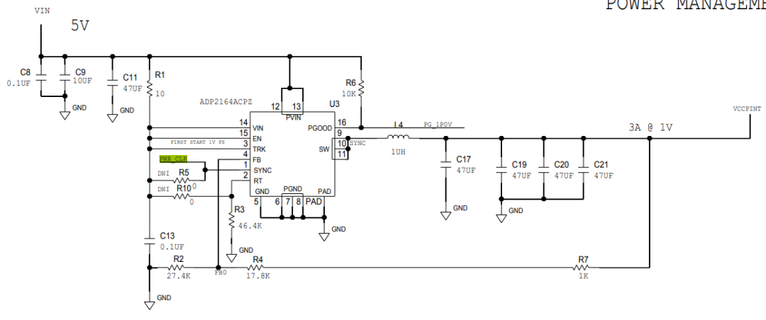
The above two images are fromRevB, mainly showing theADP2114ACPZ chip’sPWR_CLK signal, which is connected to theADP2164ACPZ chip’sSYNC pin. The former chip is responsible for supplying1V8 and 1V35, while the latter is responsible for supplyingVCCPINT, which is1P0V.
It is important to note that, in addition to connecting toPWR_CLK, aR85 resistor was added, connecting directly fromVIN to theADP2114ACPZ chip.
Point 4:
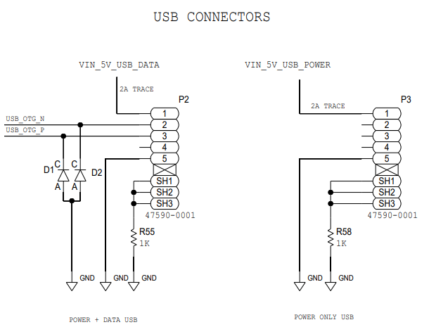
InRevA, the twoUSB ports were basically not connected to anything; the pure power port only led out the previously mentionedVIN_5V_USB_POWER power pin. The other data+ power port, in addition to leading outVIN_5V_USB_DATA power pin, also led outUSB_OTG_N and USB_OTG_P, which are the two data lines that connect to theUSB3320C USB PHY chip, and then connect to theZYNQ PS section.
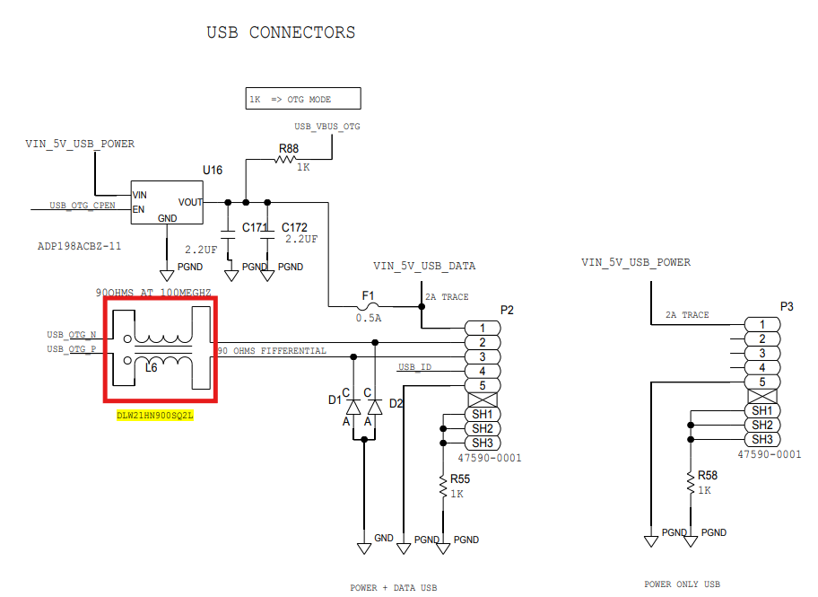
InRevB, aDLW21HN900SQ2L 90 ohm choke was connected in series on the USB differential data line.
Point 5:
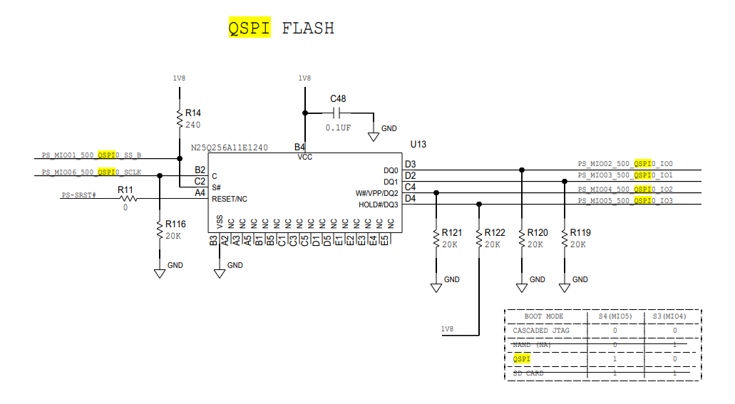
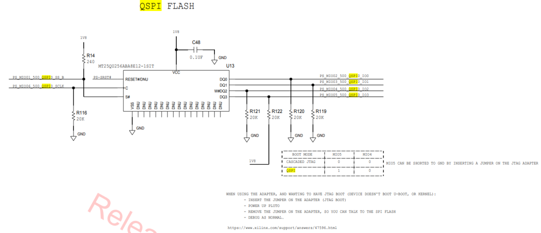
It can be seen that theFLASH chip model has changed; both models are Micron’sserial nor flash memory. TheQSPI is the bus used by theFLASH chip, which is a faster bus thanSPI. Similar toSPI, it has a chip selectCS and a clockCLK, as well as data lines. UnlikeSPI, it has multiple data lines, and each line supports bidirectional transmission. Additionally, the lower right corner ofRevB also teaches how to switch the boot mode, as seen in the upper right corner table ofRevA, where the official version consideredSD card booting.
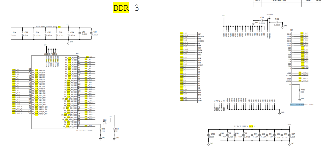
In the above image, it can be seen that theMT41K256M16TW DDR3L SDRAM chip is used, but I checked the schematics ofRevA andRevB and found that there was no change.
Point 6:
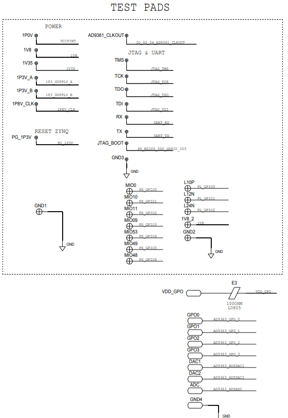
Additional test points were added, including power,JTAG, serial port,AD936x clock output, andAD/DA,ZYNQ PS andPL GPIO etc.
Among them, the power1P0V 1V8 1V35 1P3V_A 1P3V_B can be connected out for power timing verification.
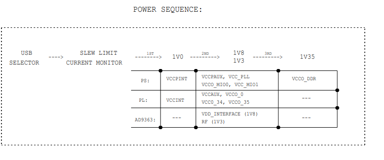
The timing in the above image is ideal and can be compared with actual measurements. The table in the above image also provides information on the different parts of the chip, indicating which power rail is used for power supply, such as1V35 supplying power toDDR related chips.
Point 7:
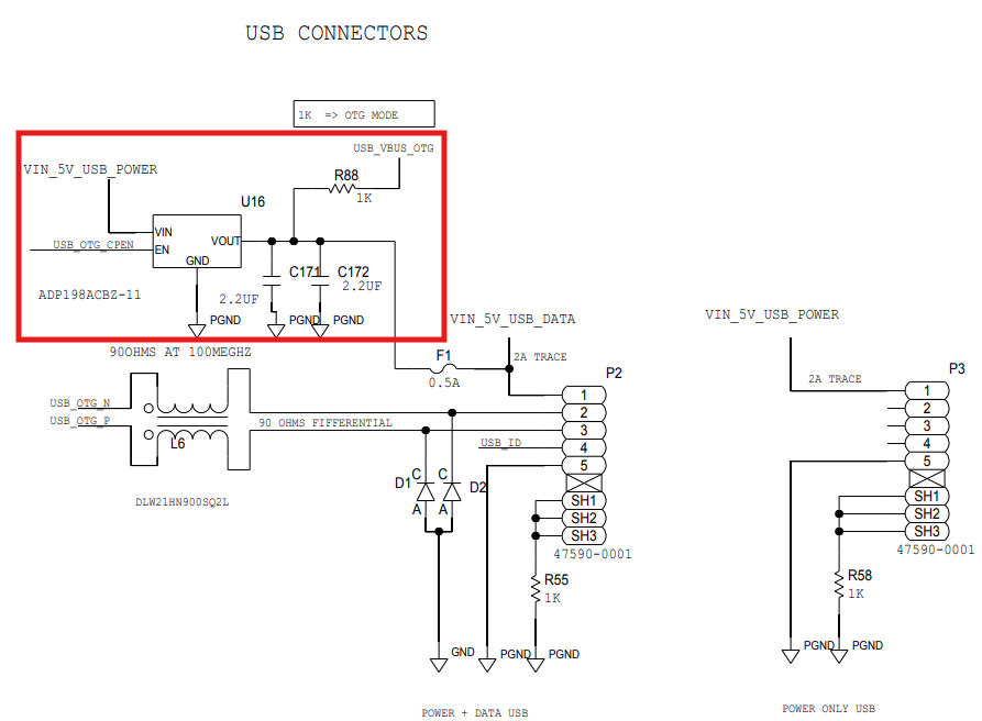
To enhanceOTG, the circuit in the red circle above was added. Theadp198acbz-11 chip is used to prevent current from flowing from the output to the input. However, theR88 resistor in this section has issues, and changes will be made in the next version.