Renesas Electronics, a leading semiconductor manufacturer in Japan, was established in 2010 and focuses on chip research and production in the automotive electronics, industrial, and IoT sectors. As of 2023, its automotive business accounts for 47%, covering core products such as microcontrollers (MCUs) and power semiconductors, with a global market share of 27.9%, ranking first in the MCU market.
1. Analysis of the Background of Renesas Electronics’ Exit from the Silicon Carbide Market
At the end of May 2025, Japanese semiconductor giant Renesas Electronics announced the termination of its silicon carbide (SiC) power semiconductor production plan, disbanding the SiC chip production team at its Takasaki plant in Gunma Prefecture, marking the complete abandonment of a project originally scheduled to commence production in early 2025. This decision reflects the structural adjustments and intense competition currently experienced in the global silicon carbide industry, driven by three key factors:
Global market demand fluctuations: The decline in electric vehicle subsidies in several European countries has led to a slowdown in market growth. The SiC market size is expected to grow only 18% in 2024, reaching 391 billion yen (approximately 2.69 billion USD), far below the previously forecasted growth rate of 27% and a market size of 491.5 billion yen. As the world’s largest market for new energy vehicles, China has also seen a general cooling in demand, further exacerbating the supply-demand imbalance for upstream silicon carbide devices. A report by Fuji Economic Research clearly indicates that the slower-than-expected growth in demand for automotive SiC chips is the main reason for the market downgrade, particularly in core application areas such as main drive inverters.
Price pressure from Chinese companies: Chinese silicon carbide companies, leveraging localized supply chain advantages, have demonstrated strong competitiveness in product pricing. Domestic manufacturers such as Tianjiao HeDa and Sanan Integrated have captured 70% of the market share in conductive substrates in China and continue to reduce cost structures through capacity expansion. Renesas found in its assessment that if it proceeded to mass production as originally planned, it would inevitably be drawn into a fierce price war with Chinese manufacturers, which the high-cost structure of Japanese companies could not sustain.
Concentration of supply chain risks: Renesas’ core SiC wafer supplier, Wolfspeed, has fallen into financial crisis and is considering filing for bankruptcy. This event poses significant recovery risks for the $2 billion (approximately 143.99 billion RMB) advance payment previously made by Renesas, becoming the last straw that broke the camel’s back. The predicament of Wolfspeed, a global leader in SiC substrates (with a 60% market share), reveals the operational fragility of the entire industry under the mismatch between capacity expansion and market demand.
Renesas’ exit decision reflects the limitations of Japanese semiconductor companies in strategic adjustments: Faced with the high risks and investments associated with technological iterations, as well as the price advantages of Chinese manufacturers supported by policy and scale effects, traditional giants have opted for tactical withdrawal due to insufficient strategic depth. This event also signals that the global silicon carbide industry will enter a period of deep integration, where companies lacking a full industry chain layout or cost control capabilities will face greater pressure.
2. International Competitive Landscape and Capacity Layout

The global silicon carbide industry has formed a competitive landscape with the US, Europe, and Japan as technology leaders and China as a fast follower. According to the ranking of the most promising companies in the global silicon carbide industry for 2025, leading companies are building their respective moats through differentiated positioning and technological routes.
2.1 Strategic Layout of Regional Leading Enterprises
Table: Analysis of Competitive Layout of Major Global Silicon Carbide Manufacturers

US technology leading route: Centered around Wolfspeed, its 8-inch substrate mass production technology can reduce costs by 30% and occupies a core position in the Tesla supply chain. Despite facing financial pressures, the company is actively promoting the construction of a 200mm device factory in Saarland, Germany, which is part of the “Important Project of Common European Interest” (IPCEI) and employs innovative sustainable development measures. Once fully operational, it will employ over 600 people. Onsemi focuses on the photovoltaic sector, leveraging a 20% cost advantage over peers to become the largest global supplier of photovoltaic SiC.
European automotive companies’ deep binding model: STMicroelectronics (ST) occupies 35% of the automotive-grade SiC device market through partnerships with over 20 global automotive companies, including Tesla and ZF. Its strategic focus is shifting to Asia, where it has established an 8-inch device factory in Chongqing in a joint venture with Sanan Optoelectronics, with Sanan holding the majority stake and building a 7 billion RMB substrate factory to form a localized closed-loop supply system. Infineon is deepening its cooperation with Bosch and Volkswagen, driven by the EU’s “carbon neutrality” policy, to strengthen its advantages in automotive-grade modules.
Japan focuses on niche markets: ROHM is the only company globally to achieve mass production of all-SiC modules. Although it faces its first net loss in 12 years due to excessive investment in fiscal year 2024, it maintains a deep partnership with Toyota. Toshiba Semiconductor focuses on the rail transportation sector, providing exclusive SiC modules for Shinkansen trains and achieving a 200% increase in orders for Southeast Asia high-speed rail projects.
2.2 The Rise of Chinese Manufacturers and Global Impact

Chinese silicon carbide companies have achieved rapid breakthroughs with policy support and market advantages, reshaping the global supply chain landscape:
Full industry chain layout breakthroughs: Sanan Integrated, as the largest IDM model enterprise in China, covers the entire chain from crystal growth to substrate, epitaxy, chip, and packaging. Its Hunan base has secured a supply of 500,000 pieces/year of 6-inch capacity for 2023-2024. Tianyue Advanced occupies 30% of the global semi-insulating substrate market and has close cooperation with Huawei and SMIC.
Differentiated competition in niche fields: TAIKO Tianrun occupies 40% of the SiC module market for charging piles in China, deeply binding with the State Grid; Silan Microelectronics holds a 50% market share in the home appliance SiC module market, serving leading customers such as Midea and Gree. Aisiter is one of the first manufacturers in China to mass-produce SiC MOSFET devices, with a full range of SiC MOSFET and module products, and has obtained automotive-grade SiC module certification.
Price pressure from capacity expansion: The large-scale capacity construction by Chinese companies is expected to lead to a 20% drop in SiC market prices in 2024, directly impacting the profit expectations of companies like Renesas. According to internal assessments at Renesas, the localized supply chain of Chinese manufacturers allows them to maintain a cost structure that is over 30% lower than that of Japanese companies, which has become a key factor forcing Renesas to exit.
3. Manufacturing Technical Difficulties and Challenges

The manufacturing of silicon carbide devices faces multidimensional challenges from material properties to process technologies, which constitute high barriers to entry for the industry and are key factors affecting the industrialization process.
3.1 Basic Limitations from Material Properties
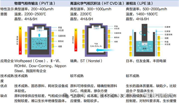
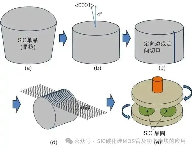
Crystal growth bottlenecks: SiC crystals need to grow in a high-temperature closed environment above 2000°C, requiring extremely high temperature control precision. Silicon material can complete crystal growth in an average of only 3 days, while the growth cycle for silicon carbide crystals can take up to 7 days, with low output efficiency—silicon crystals can grow up to 200 cm, while SiC crystals can only grow about 2 cm. More complex is that SiC has over 200 types of crystal structures, but only a few (such as 4H-SiC) are suitable for semiconductor materials, requiring precise control of multiple parameters such as silicon-carbon ratio, temperature gradient, and growth rate.
Wafer processing difficulties: SiC has a Mohs hardness of 9.2, second only to diamond, leading to a high scrap rate during cutting, grinding, and polishing processes. The edge chipping problem caused by traditional mechanical cutting severely affects yield, and the warping phenomenon of thinned wafers is much more serious than that of silicon wafers. According to production line measurement data, the scrap rate of SiC wafers during thinning can be more than three times that of silicon-based semiconductors, significantly increasing manufacturing costs.
Epitaxy quality control: High-voltage SiC devices require the thickness of the epitaxial layer to increase with the voltage rating—600V devices need a 6μm epitaxial layer, while 1700V devices require 10-15μm, and devices above 10kV may even need a thickness of 100μm. As the thickness increases, controlling resistivity uniformity and defect density becomes extremely difficult. Currently, epitaxy equipment is monopolized by four giants: Axiotron, LPE, TEL, and Nuflare, further restricting the autonomy of the industry chain.
3.2 Process Manufacturing Costs and Industrialization Challenges
Special process requirements: Due to the material properties of SiC, traditional silicon-based processes cannot be directly migrated:
①Doping process: SiC cannot achieve doping through thermal diffusion and must use high-energy ion implantation (300-700keV), combined with high-temperature annealing above 1700°C, which places extremely high demands on equipment temperature resistance and stability.
②Gate oxide process: During high-temperature oxidation, carbon atoms react to form impurity interface states, leading to a decrease in electron mobility, necessitating the development of atomic-level interface control technologies.
③Etching technology: SiC is inert to chemical solvents and must use dry etching, but challenges such as mask material selection, sidewall slope control, and surface roughness optimization have not yet been fully overcome.
Device design challenges: Planar SiC devices, while simpler in process, suffer from JFET effects that increase conduction resistance; trench-type structures can reduce chip area (e.g., ROHM’s Gen3 chips are 25% smaller than Gen2) and lower conduction resistance by 50%, but face trade-offs in unit consistency and process complexity. Additionally, SiC power modules are highly sensitive to parasitic capacitance and inductance, and high switching speeds can lead to overshoot and oscillation, making traditional silicon-based packaging structures inadequate.
Cost structure imbalance: In SiC devices, the substrate accounts for as much as 47% of the cost, and the epitaxy accounts for 23%, with both together making up 70% of the value chain. Compared to international leading levels, the cost share of substrates for Chinese companies is even higher, reaching 50-60%. Currently, the price of international SiC devices is still 5-6 times that of silicon-based products, although it is decreasing at a rate of 10% per year, it will still take 2-3 years to reach the replacement critical point (2-3 times that of silicon-based products). Yield issues are particularly prominent—6-inch SiC wafers generally have a yield of 60-70%, far below the 90% or more of silicon-based semiconductors, becoming the biggest obstacle to cost reduction.
4. Technological Breakthroughs and Industrial Strategies
Faced with technological and industrialization challenges, the global silicon carbide industry is seeking breakthroughs from multiple dimensions, including technological path innovation, industrial chain model reconstruction, and policy collaboration.

4.1 Technological Evolution Path
Transition to large-diameter wafers: The shift from 6-inch to 8-inch wafers has become a key path for cost reduction. Sanan Optoelectronics and STMicroelectronics’ Chongqing joint venture factory focuses on the 8-inch line, with research indicating that this wafer size can increase the yield of qualified chips by 80%-90% and reduce overall costs by 15%. The 8-inch wafers, due to their increased thickness, can better maintain geometric shape and reduce edge warping, thereby lowering defect density. The 200mm factory being built by Wolfspeed in Saarland, Germany, will adopt innovative manufacturing processes and become the largest silicon carbide device manufacturing base globally.
Trench structure innovation: ROHM’s third-generation trench structure (Gen3 Trench) reduces conduction resistance by 50% at the same chip size by optimizing cell density, shrinking the chip area to 75% of the previous generation. Infineon has introduced CoolSiC™ MOSFET trench gate technology, achieving higher switching frequencies at the same conduction loss, particularly suitable for electric vehicle main drive inverter applications.
Advanced packaging integration: In response to the high switching speed characteristics of SiC, the industry has developed wireless interconnection and double-side cooling technologies, significantly reducing parasitic parameters. STMicroelectronics has replaced bonding wires with copper clamps in the Tesla Model 3 main drive module, reducing thermal resistance by 60% and improving power cycling capability by five times. Intelligent power modules (IPM) that integrate driver ICs, temperature sensors, and decoupling capacitors are also accelerating in popularity, with Mitsubishi Electric applying this technology in air conditioning variable frequency modules, achieving the highest global market share.
Defect control technologies: Soitec’s SmartCut™ technology improves substrate yield by 20% through ion cutting and bonding processes, providing a key technological path for 8-inch SiC mass production. Tianyue Advanced in China has developed a “multi-step epitaxy method” that controls defect density to below 0.5/cm² in epitaxial layers thicker than 100μm, meeting the requirements for 10kV-level devices.
4.2 Industrial Chain Restructuring Strategies
Vertical integration model: Sanan Optoelectronics has pioneered a dual-track model of “wholly-owned substrates + joint venture devices,” investing 7 billion RMB in Chongqing to build an 8-inch substrate factory, exclusively supplying the joint venture device factory with STMicroelectronics, achieving closed-loop management of the entire industry chain. This model ensures material security while enhancing international recognition through technological cooperation. Wolfspeed adheres to the IDM model from substrate to module, utilizing its global largest silicon carbide crystal growth factory in North Carolina to achieve collaborative optimization from materials to devices.
International capacity collaboration: In the face of geopolitical risks, leading companies are accelerating the construction of diversified supply chains. The $3.2 billion joint venture project between STMicroelectronics and Sanan Optoelectronics introduces technology into local production in China, avoiding trade barriers and shortening delivery cycles to Asian customers. ZF’s “significant investment” in Wolfspeed’s German factory reflects the strategic intent of automotive companies to extend upstream and secure core device supplies.
Application scenario innovation: In the context of short-term pressure in the automotive market, leading companies are actively exploring new growth points:
Photovoltaic sector: Onsemi has launched dedicated SiC solutions that break inverter conversion efficiency above 99%, reducing system losses by over 50%, and has captured the top position in the global photovoltaic SiC market.
Fast charging applications: TAIKO Tianrun has developed customized modules for the Chinese charging pile market, in conjunction with the State Grid’s ultra-fast charging network, achieving a market share of 40%. Wolfspeed’s 220kW full-bridge resonant LLC solution reduces charger size by 25%, achieving peak efficiency of 98.3%.
High-temperature scenarios: Mitsubishi Electric has developed SiC IPM modules specifically for air conditioning compressors, leveraging their high-temperature resistance characteristics to meet global air conditioning energy efficiency standard upgrades, achieving the highest global market share.
4.3 Policy and Ecological Collaboration
Government strategic support: The EU has included Wolfspeed’s German factory in the “Important Project of Common European Interest” (IPCEI), granting exemptions from national aid rules. China’s “new infrastructure” policy drives capacity expansion for companies like Sanan Integrated, allowing China’s automotive SiC self-sufficiency rate to exceed 50%. The US “CHIPS Act” provides special subsidies for domestic SiC research and development, supporting companies like Cree in their technological upgrades.
Cross-industry alliance building: ZF and Wolfspeed are collaborating to build a joint research and development center for silicon carbide in Germany, jointly developing automotive-grade modules under the IPCEI framework.
Cost balance strategies: In response to the system cost advantages of SiC devices, the industry promotes a “Total Cost of Ownership” (TCO) assessment model. STMicroelectronics calculates that using SiC MOSFETs in electric vehicles increases costs by about $300, but can save up to $2000 in system costs by improving efficiency, reducing battery usage, and simplifying cooling systems. ROHM’s analysis indicates that a 3%-5% increase in SiC inverter efficiency can significantly reduce battery capacity requirements, positively impacting overall vehicle costs and weight.
5. Conclusion: A Development Outlook of Coexisting Challenges and Opportunities
Renesas Electronics’ exit from the silicon carbide market marks the beginning of a deep adjustment period for the industry, but this is not a failure of the technological route, rather a structural optimization in the process of industrial development. In the short term, the mismatch between slowing market growth (only 18% growth in 2024) and capacity expansion will bring growing pains, with some companies facing financial pressures or even exiting. However, in the long term, driven by core forces such as electric vehicles and renewable energy, Yole predicts that the compound annual growth rate of the silicon carbide power device market will still reach 31% from 2022 to 2028, with a market size of $8.9 billion by 2028.
The next three years will be a critical watershed for the industry, where technological breakthroughs and industrial integration will reshape the competitive landscape:
Technological dimension: Mass production of 8-inch wafers, popularization of trench structures, and breakthroughs in defect control technology are expected to reduce SiC device costs to 2-3 times that of silicon-based products by 2027, triggering a large-scale replacement critical point.
Industrial landscape: The IDM model and regional collaboration will become mainstream, with Chinese companies potentially capturing over 40% of the global supply chain share under policy support and capacity advantages.
Application scenarios: The main drive inverter for electric vehicles remains the largest market, but the penetration rates in photovoltaic inverters, data center power supplies, and industrial motors will increase from 15% in 2025 to 45% by 2030.
In this industrial transformation, the success of enterprises will depend on the depth of technological innovation, the ability to integrate the industrial chain, and the collaborative advancement of application scenario expansion. Participants who can break through material limits, reconstruct cost boundaries, and accurately position the market will lead a new industrial order in the “post-Renesas era” of silicon carbide. The rise of Chinese companies is changing the previously US, European, and Japanese-dominated competitive landscape, driving the global silicon carbide industry towards diversification and regionalization.
Note: This article is sourced from the internet and is intended to convey more information. The views expressed in the article are for sharing and communication purposes only and do not represent the position of this public account. Please indicate the source when reprinting. If there are any errors in source attribution or if there are copyright issues, please contact us, and we will correct or delete it promptly. Thank you.
 Focused on the research and application of silicon carbide devices. Sharing industry information on the design, research and development, and application of silicon carbide devices.To join the communication WeChat group, please add personal WeChat: 18126115420, and note your company + name + research direction.