Fundamentals of Semiconductor Materials
Semiconductor materials are electronic materials used to make semiconductor devices and integrated circuits, forming the foundation of the semiconductor industry. The various semiconductor devices and integrated circuits made from semiconductor materials have accelerated the rapid development of modern information society.
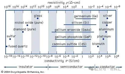
Figure 1: Typical conductivity ranges of insulators, semiconductors, and conductors
The research on semiconductor materials began in the early 19th century.
Elemental semiconductors are those composed of a single type of atom, such as silicon (Si), germanium (Ge) from group IV of the periodic table, and selenium (Se) and tellurium (Te) from group VI. However, there are many compound semiconductors made of two or more elements. For example, gallium arsenide (GaAs) is a binary III-V compound formed by combining gallium (Ga) from group III and arsenic (As) from group V. Ternary compounds can be formed from elements from three different groups, such as mercury indium telluride (HgIn2Te4), a II-III-VI compound. They can also be formed from elements from two groups, such as aluminum gallium arsenide (AlxGa1-xAs), a ternary III-V compound where both Al and Ga come from group III, and the subscript x relates to the composition of the two elements from 100% Al (x = 1) to 100% Ga (x = 0).
Pure silicon is the most important material in integrated circuit applications, while binary and ternary III-V compounds are crucial for optoelectronics.
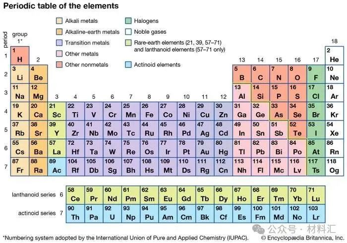
Figure 2: Periodic Table of Elements
Before the invention of the bipolar transistor in 1947, semiconductors were only used as two-terminal devices, such as rectifiers and photodiodes. In the early 1950s, germanium was the primary semiconductor material. However, it turned out that this material was unsuitable for many applications because devices made from it exhibited high leakage currents only at moderately elevated temperatures. Since the early 1960s, silicon has become the most widely used semiconductor, effectively replacing germanium as the material for device manufacturing. The main reasons for this are twofold: (1) the leakage current of silicon devices is much lower, and (2) silicon dioxide (SiO2) is a high-quality insulator that can be easily integrated as part of silicon-based devices. Consequently, silicon technology has become highly advanced and widespread.
The Development Path of Semiconductor Materials
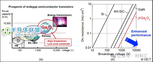
Figure 3: The Development Path of Semiconductor Materials and Comparison of Different Materials
First Generation Semiconductor Materials: Silicon (Si), Germanium (Ge)
In the history of semiconductor material development, prior to the 1990s, silicon materials dominated as the first generation of semiconductor materials. Currently, semiconductor devices and integrated circuits are still primarily manufactured using silicon crystal materials, which account for over 95% of all semiconductor products sold globally. The development of silicon semiconductor materials and their integrated circuits has led to the emergence of microcomputers and a leap in the entire information industry.
Second Generation Semiconductor Materials: Gallium Arsenide (GaAs), Indium Phosphide (InP)
With the rise of information highways based on optical communication and the development of social informatization, second-generation semiconductor materials represented by gallium arsenide and indium phosphide have emerged, demonstrating their significant advantages. Gallium arsenide and indium phosphide semiconductor lasers have become key components in optical communication systems, while gallium arsenide high-speed devices have also opened up new industries in fiber optics and mobile communications.
Third Generation Semiconductor Materials: Gallium Nitride (GaN), Silicon Carbide (SiC)
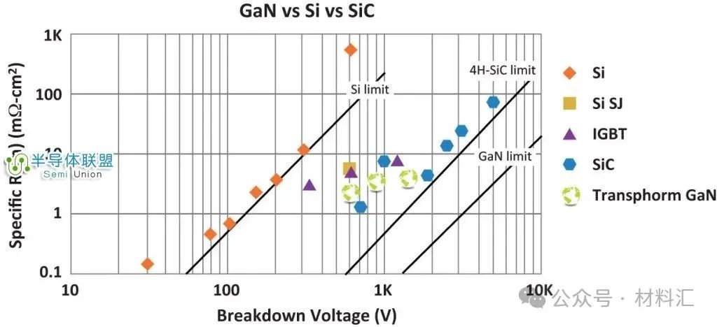
Figure 4: Comparison of GaN with Si and SiC
The rise of third-generation semiconductor materials began with breakthroughs in P-type doping of gallium nitride materials, marked by the successful development of high-efficiency blue-green light-emitting diodes and blue semiconductor lasers, indicating vast application prospects in light display, optical storage, and lighting.
Third-generation semiconductor materials, represented by gallium nitride and silicon carbide, possess excellent properties such as high breakdown electric field, high thermal conductivity, high electron saturation velocity, and strong radiation resistance, making them more suitable for manufacturing high-temperature, high-frequency, radiation-resistant, and high-power electronic devices. They are the “core” of solid-state light sources, power electronics, and microwave RF devices, with broad application prospects in semiconductor lighting, the next generation of mobile communications, energy internet, high-speed rail transportation, new energy vehicles, and consumer electronics. They are expected to break through the bottlenecks of traditional semiconductor technology, complementing first and second-generation semiconductor technologies, and playing a significant role in energy conservation, emission reduction, industrial transformation and upgrading, and fostering new economic growth points.
Third-generation semiconductor materials are currently a new strategic competitive high ground globally and a key industry supported by our country. During the 12th Five-Year Plan period, the 863 Program focused on supporting projects related to the “Preparation and Evaluation Technology of Third-Generation Semiconductor Devices.”
Fourth Generation Semiconductor Materials: Gallium Oxide (Ga2O3)
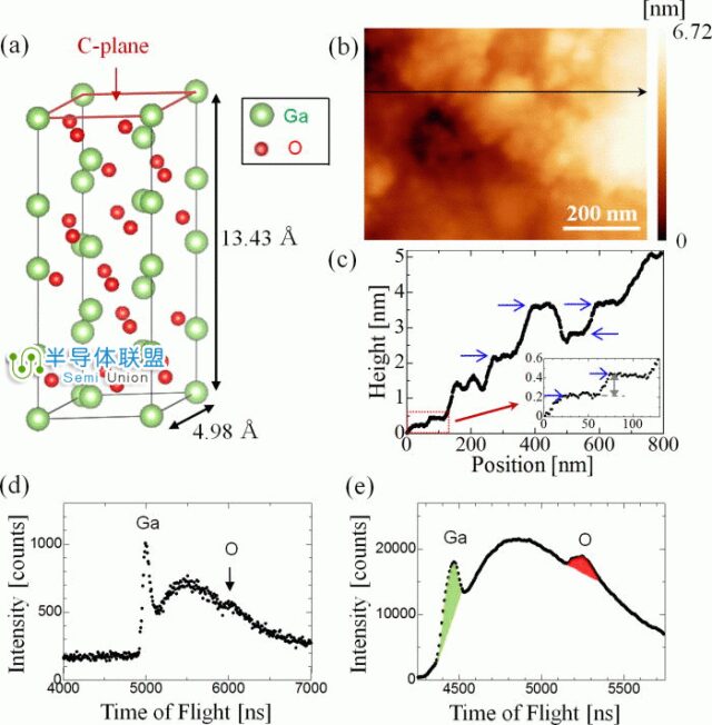
Figure 5: Structure and Atomic Force Microscopy Image of Gallium Oxide (Ga2O3)
As a new type of wide-bandgap semiconductor material, gallium oxide (Ga2O3) has attracted increasing attention and research due to its excellent properties, boasting a wider bandgap than third-generation semiconductor materials SiC and GaN. It has broad application prospects in ultraviolet detection and high-frequency power devices. Gallium oxide is a wide-bandgap semiconductor with a bandgap width of Eg=4.9eV, good conductive and luminescent properties, making it widely applicable in optoelectronic devices, used as an insulating layer for Ga-based semiconductor materials and ultraviolet filters. These are traditional application areas for gallium oxide, while its future applications in power, especially high-power scenarios, are even more promising.
There is a rich variety of semiconductor materials, and in addition to the typical materials mentioned above, there are organic semiconductors, ceramic semiconductors, and others, each possessing unique properties and applications.
Electronic Properties of Semiconductor Materials
The semiconductor materials described here are single crystals; that is, the atoms are arranged in a three-dimensional periodic manner. Part A of this figure shows a simplified two-dimensional representation of intrinsic (pure) silicon crystals containing negligible impurities. Each silicon atom in the crystal is surrounded by four nearest neighbors. Each atom has four electrons in its outer shell, sharing these electrons with its four neighbors. Each shared electron pair constitutes a covalent bond. The attraction between electrons and the two atomic nuclei holds the two atoms together. For isolated atoms (for example, in gases rather than in crystals), electrons can only have discrete energy levels. However, when a large number of atoms come together to form a crystal, the interactions between the atoms cause the discrete energy levels to spread into energy bands. When there is no thermal vibration (i.e., at low temperatures), the electrons in the insulator or semiconductor crystal will completely fill several energy bands, while the remaining bands will be empty. The highest filled band is called the valence band. The next energy band is the conduction band, which is separated from the valence band by a bandgap (the gap in a crystal insulator is much larger than that in a semiconductor). This bandgap is also known as the energy gap, which designates the range of energies that electrons in the crystal cannot possess. The bandgap of most important semiconductors ranges from 0.25 to 2.5 electron volts (eV). For example, silicon has a bandgap of 1.12eV, and gallium arsenide has a bandgap of 1.42eV. In contrast, the bandgap of a good crystal insulator like diamond is 5.5 eV.
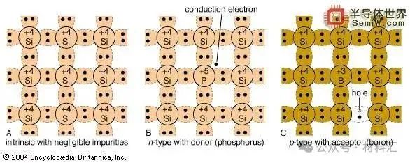
Figure 6: Three-Bond Image of Semiconductors
At low temperatures, electrons in semiconductors are bound within their respective energy bands in the crystal. Therefore, they are not available for conduction. At higher temperatures, thermal vibrations may break some covalent bonds, creating free electrons that can participate in current conduction. Once an electron breaks free from a covalent bond, that bond will have an electron vacancy. This vacancy can be filled by an adjacent electron, causing the vacancy to move from one crystal site to another. This vacancy can be considered a fictitious particle called a “hole,” which carries a positive charge and moves in the opposite direction to the electron. When an electric field is applied, both the free electrons (now in the conduction band) and holes (left behind in the valence band) move through the crystal, generating current. The conductivity of the material depends on the number of free electrons and holes (charge carriers) per unit volume, as well as the rate at which these carriers move under the influence of the electric field. In intrinsic semiconductors, there are equal numbers of free electrons and holes. However, electrons and holes have different mobilities. That is, they move at different speeds in the electric field. For example, for intrinsic silicon at room temperature, the electron mobility is 1,500 square centimeters per volt-second (cm²/V·s), meaning that electrons will move at 1,500 centimeters per second under an electric field of 1 volt/centimeter—while the hole mobility is 500 cm²/V·s. The electron and hole mobilities in a specific semiconductor typically decrease with increasing temperature.
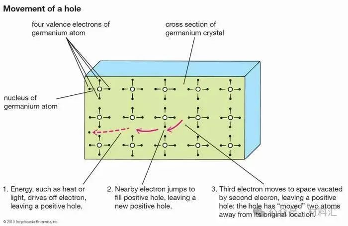
Figure 7: Motion of Electron Holes in the Lattice
At room temperature, intrinsic semiconductors have very poor conductivity. To achieve higher conductivity, impurities can be deliberately introduced (usually reaching concentrations of a few parts per million of the main atom). This process is known as doping, which, although it increases some mobilities, still enhances conductivity. For example, if a silicon atom is replaced by an atom with five outer-layer electrons, such as arsenic (as seen in part B of the figure), four electrons form covalent bonds with four neighboring silicon atoms. The fifth electron becomes a conductive electron provided to the conduction band. Silicon becomes an n-type semiconductor due to the addition of electrons. Arsenic atoms are donors. Similarly, part C of the figure shows that if an atom with three outer electrons (such as boron) replaces a silicon atom, an additional electron will be accepted to form four covalent bonds around the boron atom, creating a positively charged hole in the valence band. This results in a p-type semiconductor, where boron acts as an acceptor.
If there is a sharp change in the type of impurity, from acceptor (p-type) to donor (n-type) within a single crystal structure, a p-n junction is formed (see parts B and C of the figure). On the p-side, holes are the majority carriers, thus referred to as majority carriers. There will also be some thermally generated electrons present, known as minority carriers. On the n-side, electrons are the majority carriers, while holes are the minority carriers. Near the junction is a region devoid of free charge carriers, known as the depletion region, which behaves as an insulator.
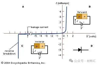
Figure 8: (A) Current-Voltage Characteristics of a Typical Silicon p-n Junction (B) Forward Bias (C) Reverse Bias Conditions (D) Symbol of p-n Junction
Source: Semiconductor Alliance
Introduction to the Promotion Association
Guangzhou New Materials Industry Development Promotion Association is a professional new materials industry service organization with independent legal status, initiated by key enterprises such as Jinfat Technology, Guangzhou Automation (formerly Guanggang Group, Wanli Group), Provincial Academy of Sciences Chemical Institute, China National Measurement, Qingtian Materials, Tianci Materials, Guangzhou Chemical Reagent Factory, Aoyi Electronics, and Huari Optoelectronics under the guidance of the Guangzhou Municipal Bureau of Industry and Information Technology. It was registered in October 2017 with the Municipal Civil Affairs Bureau. The current president unit is Guangdong-Hong Kong-Macao Greater Bay Area Huangpu Materials Research Institute.
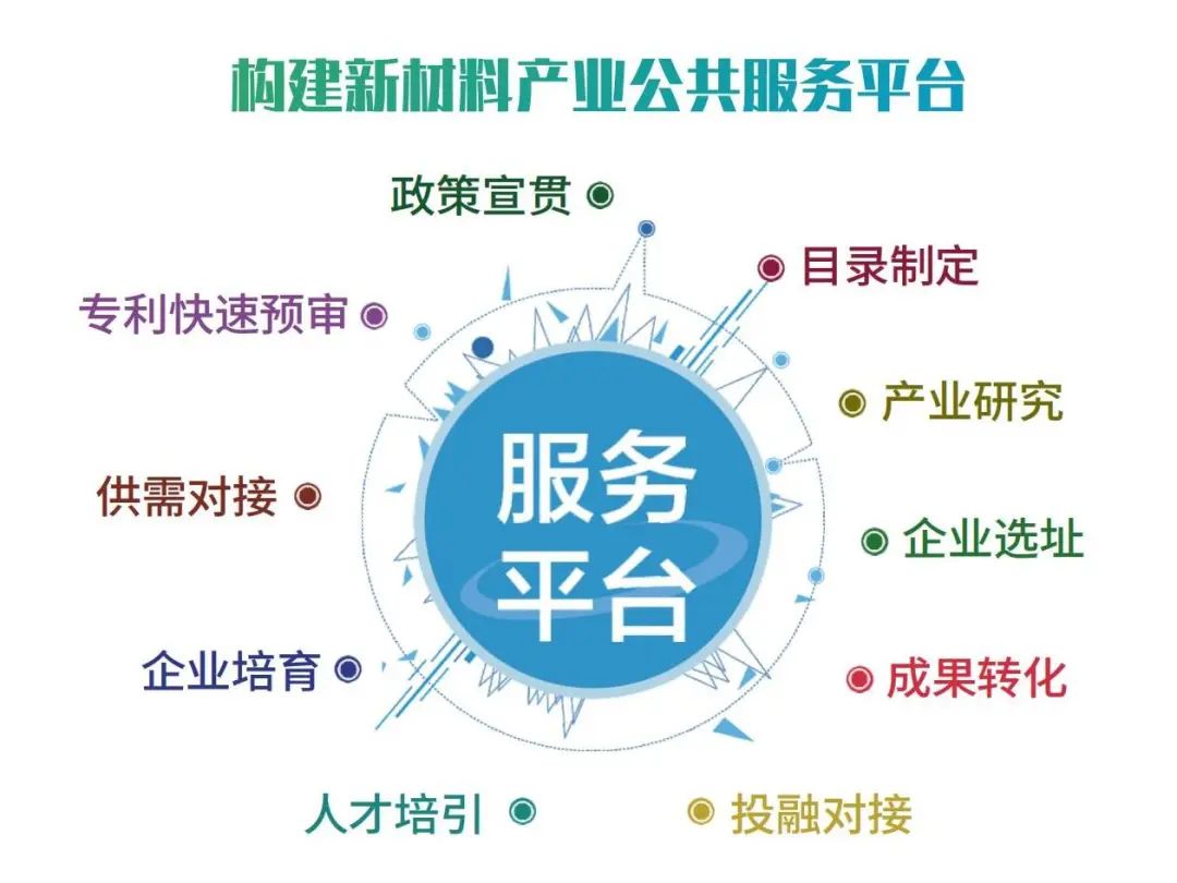
The association is committed to promoting the high-quality development of the new materials industry, focusing on advanced petrochemicals, automotive materials, electronic materials, pharmaceutical materials, and cutting-edge new materials, providing services such as policy dissemination, directory formulation, industry research, enterprise site selection, achievement transformation, investment and financing docking, talent training, enterprise cultivation, supply and demand docking, and rapid patent pre-examination, establishing a public service platform for the new materials industry. Since its establishment, the association has organized over 60 specialized seminars with experts in the new materials subfields, hosted more than 120 various industry exchange activities, established a think tank of experts in the new materials industry cluster, and served and engaged with thousands of enterprises, assisting the Municipal Bureau of Industry and Information Technology and other competent authorities in conducting research on green petrochemicals and the new materials industry, regional industrial planning, compiling the first batch of directories for key new materials, and developing new materials industry clusters. It has received honors such as the Guangzhou Federation of Industry and Commerce Group Membership, Guangzhou General Chamber of Commerce Group Membership, New Materials Industry Cluster Intellectual Property Service Station, and the Guangzhou Council for the Promotion of International Trade New Materials Industry Committee, contributing to the high-quality development of the new industrialization sector.


Public Email of the Secretariat:
Membership or Inquiry Phone:
020-83522271
Contact Address:
Room G, 10th Floor, No. 448, Dongfeng Middle Road, Guangzhou