This article was originally published in the Zhihu column [The Path of Digital IC Backend Engineers].
In the field of low power design, the most effective way to reduce power consumption is through power shutdown. This is because no matter how low the voltage, how small the current, how slow the speed, or how minimal the leakage, nothing is as effective as completely turning off the power supply.
However, in practical design, the power gating design method greatly increases the complexity of the design, with many characteristics differing from general designs, from design to verification, and from backend implementation to signoff methodology.
Today, we will mainly introduce the characteristics and principles of power gating from the perspective of logical composition and backend implementation. A typical design with power gating should include the following main modules:
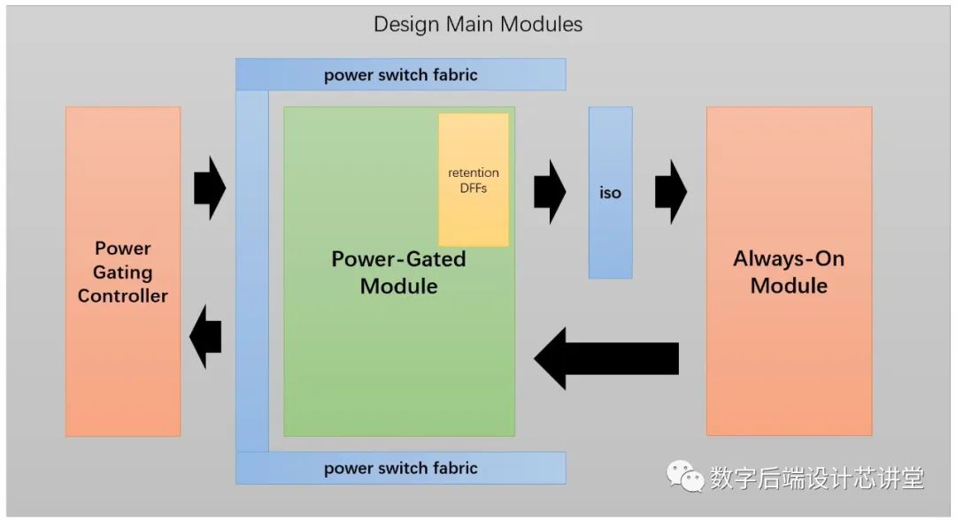
Power gating controller: Controls when to turn off the power supply to the shutdown module in the chip and provides necessary enable signals to special cells such as retention registers;
Power switching fabric: Also known as power switch, it implements the logic unit for shutting down the power supply, generally added during the backend implementation phase and placed according to specific design rules;
Always-on module: A module that keeps the power supply always on;
Isolation cells: Referred to as ISO, these cells are generally required for signals entering the always-on module from the shutdown module, and their specific function will be explained later;
Retention DFFs: Special registers that can retain data without loss when the main power supply is turned off, only needed when some data must be preserved during power shutdown.
Next, we will introduce the principles and characteristics of power gating from several aspects.
Shutdown Methods
There are mainly two shutdown methods: turning off VDD or turning off VSS, and the basic principles of both are quite simple, as shown in the figure below. In practical applications, turning off VDD is the primary method, and all the types I have encountered are of the VDD shutdown type.
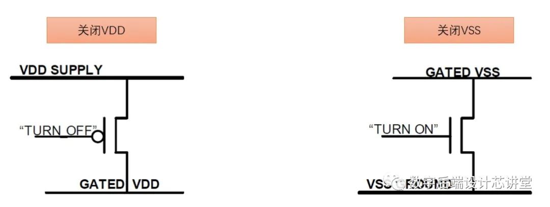
Generally, only one shutdown method is used on the same chip, meaning that there will not be a situation where part of the circuit shuts down VDD while another part shuts down VSS. As for how to implement the shutdown, this requires the use of power switch cells.
Power Switch Cells
Power switch cells are equivalent to switches in general circuits, but they are not implemented by contact switches in high-power circuits; instead, they are constructed using CMOS circuits. However, we know that the current that a MOS transistor can handle is very limited, and when shutting down one or more modules, the required current value should be relatively large. Therefore, power switch cells must work in large numbers in coordination.
There are different types of operation methods, with the following two being typical:
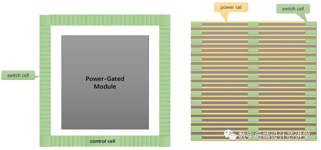
The left arrangement method places a circle or several circles of switch cells around the module that needs to be shut down and connects them end to end, with the external power supply connected to the input of the power switch and the output connected to the higher metal layer supplying power to the module, controlled by a control module to implement the power switch; the right method distributes power switch cells like standard cells according to fixed rules throughout the design, with the upper metal of the power supply connected to the input of the power switch cell, and the output connected to the power rail, achieving power shutdown by disconnecting the rail from the upper metal.
The left power switch cell arrangement is similar to the arrangement of IOs, but its size is generally larger than that of standard cells but smaller than IOs; the right switch cell is generally about the same size as a standard cell.
In fact, the placement of power switches is not limited to these two arrangements. When the module that needs to be shut down is relatively small, a few switch cells can achieve the power on/off, and the placement of these cells does not need to be limited to a specific form, as long as the connections are correct and the power supply meets the requirements, gathering the switch cells together is also acceptable.
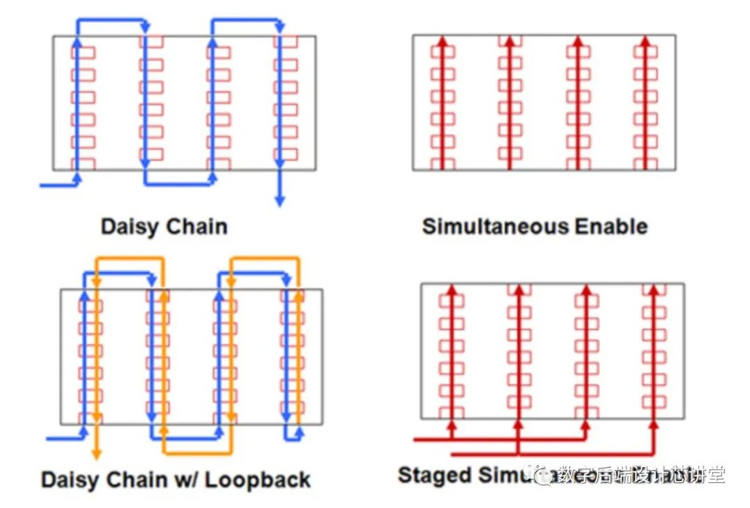
Regarding the connection methods of power switch cells, there are also different forms, which can be summarized into the following types, with the daisy chain form being the most common. Different forms of placement and connection have different characteristics in terms of response time, inrush current, IR-Drop, and area occupation, which will not be detailed here; we will explore them in another article in the future.
Isolation Cell
When a signal is transmitted from one module to another, if the power supply at the input end is turned off, the output signal may exhibit unpredictable values, which could lead to functional issues if this value is transmitted. Therefore, it is necessary to isolate the output signal of the power-off module from other modules, which requires the use of isolation cells.
The function of the isolation cell is to fix a certain signal point to a high or low potential. Its principle is quite simple, essentially equivalent to an AND or OR gate.
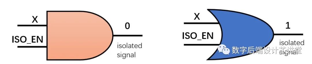
To ensure that the isolation cell can still function normally when the power is off, it generally has a primary power and a secondary power, the latter ensuring that the former can still operate when the power is turned off.
Regarding the insertion position of the isolation cell, we need to decide whether to place it within the power gated module (source) or the always-on module (destination). Since some signals from the power gated module may reach multiple different other modules, if inserted in the destination module, it may require inserting isolation cells in all destinations, leading to unnecessary resource waste. Therefore, it is generally recommended to place it within the source module.
Regardless of where it is placed, its power connections require extra attention. The placement of isolation cells must ensure that both gated power and always-on power are present and that the physical and logical connections are correct. Therefore, isolation cells are often assigned a fixed area for placement, where two different power stripes and power rails can be used to connect them, or the tools can automatically route the secondary power connection. The latter mainly occurs in non-advanced processes.
Retention Register
If certain data should not be lost during the power shutdown process, retention registers are needed to save the data. The biggest difference from general registers is that it has two different power supplies, powering a master and a slave register. When the master needs to be powered off but the data needs to be preserved, a SAVE or RETAIN signal is sent to the retention register, allowing the data to be transferred from the master to the slave register. The slave register is usually connected to the always-on power supply to ensure it can operate normally. Below are two typical constructions of retention registers:
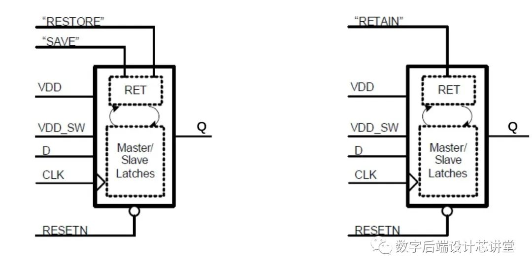
From the above structure, it can be seen that retention registers will inevitably be larger in size than general registers, generally at least 20% larger. Therefore, special attention should be paid to the additional area and power consumption brought by using retention registers. When the amount of data to be saved during power shutdown is too large, the power consumption caused by retention cells may undermine the overall low power effect.
The implementation of the above power gating and the power connections of special cells require support from UPF (Unified Power Format). Later, we will explain what content needs to be defined in UPF for typical low power designs, so stay tuned.
That concludes the introduction to multi-bit cells. If you have any questions, feel free to leave a comment for discussion~
If you have any digital backend technical topics you are interested in exploring, feel free to scan the QR code on the left to join the digital backend exchange group.
To avoid spreading advertisements, please also send verification information to answer the following question:
Besides Synopsys and Mentor, which other mainstream EDA tool vendors are there in IC design?
You are also welcome to scan the QR code on the right to follow my Zhihu:
Zhihu account : Yan Futi
Zhihu column: The Path of Digital IC Backend Design Engineers.