Chip packaging is a critical step in semiconductor manufacturing, providing physical protection, electrical interconnection, and heat dissipation for chips. Bonding technology is the method of connecting bare chips to external materials.
Currently, there are four main bonding technologies: the traditional and reliable Wire Bonding, the high-performance Flip Chip Bonding, the highly automated Tape Automated Bonding (TAB), and the future-oriented Hybrid Bonding technology.
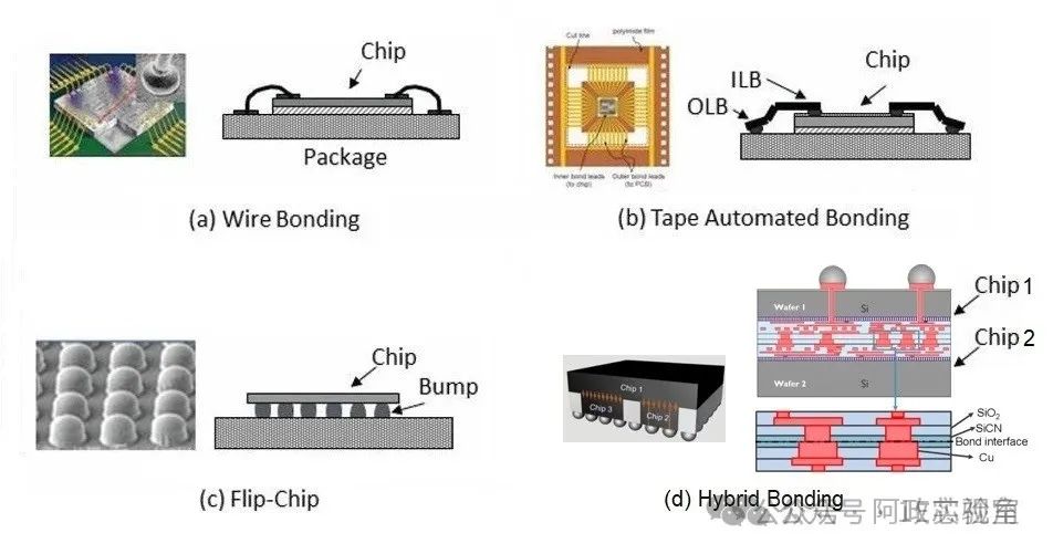
01 Wire Bonding
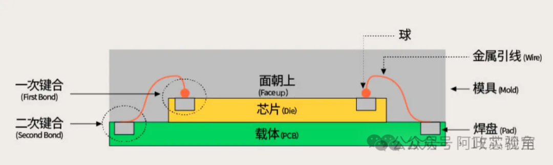
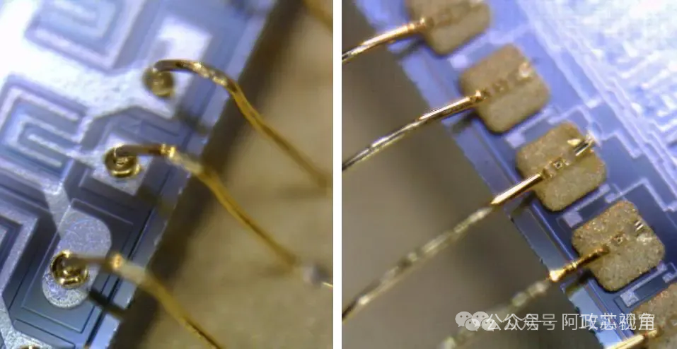
Wire bonding is the most widely used bonding technology. It utilizes heat, pressure, or ultrasound to connect the chip pads to the substrate (usually a lead frame or PCB) using fine metal wires (gold, aluminum, or copper).
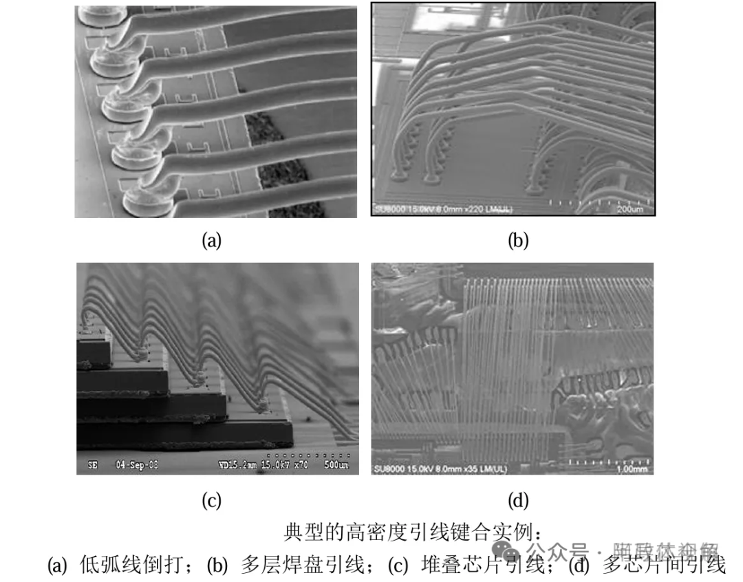
The wire bonding process requires the bonding bumps to be distributed around the edges of the chip, and the presence of wires necessitates the encapsulation to provide protection, which increases the volume and hinders heat dissipation during chip operation. As devices become smaller and more complex, the traditional wire bonding process used in packaging is gradually becoming inadequate to meet industry demands.
 1.1 Process Flow
Wire bonding mainly includes three stages: Preparation, Bonding, and Testing. The preparation involves preheating the equipment to the appropriate temperature, setting various process parameters, and loading the bonding metal wire (usually gold, copper, or aluminum).
 1.2 Bonding Methods
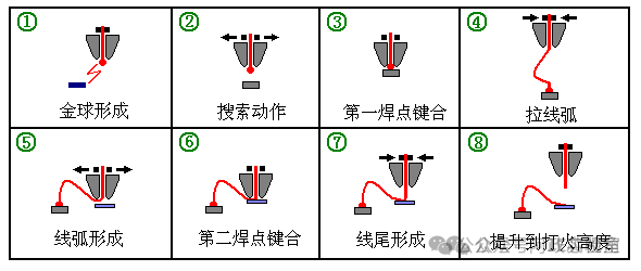
Wire bonding mainly includes Ball Bonding and Wedge Bonding, referred to as ball bonding and wedge bonding.
1.3 Bonding Mechanism
The bonding mechanism of wire bonding mainly includes Thermo-Compression Bonding (TCB), Ultrasonic Bonding, and Thermo-Sonic Bonding. Thermo-compression bonding connects the metal wire to the pad through heat and pressure, which is simple but requires high temperatures; ultrasonic bonding uses the frictional heat and mechanical action generated by ultrasonic vibrations to achieve bonding, which can be done at room temperature and allows for flexible material selection; thermo-sonic bonding uses temperature, pressure, and ultrasonic energy simultaneously, offering better process adaptability and bonding strength, making it the most widely used bonding method today.
Thermo-compression bonding (TCB) heats and presses the bump from the chip side to achieve physical connection with the substrate. The typical process temperature range for TCB is between 150ºC and 300ºC, with pressure levels between 10-200MPa. This bonding method ensures uniform adhesion without gap variations or tilting, reducing substrate warping issues (as the substrate coated with flux is firmly fixed on a vacuum plate and the overall temperature is not high), allowing I/O spacing to be reduced to smaller dimensions (around 10µm). Intel was the first to adopt substrate-based TCB technology to replace traditional reflow soldering, developed jointly by Intel and ASMPT, and introduced into mass production in 2014.
TCB technology also requires the use of a removable copper oxide flux to reduce bonding interconnect failures. However, when the interconnect spacing is reduced to below 10µm, the flux becomes more difficult to remove and leaves sticky residues, which can cause slight deformations in the interconnect, leading to corrosion and short circuits. Therefore, Kulitafaso introduced a fluxless bonding technology in 2023, operating in a vacuum or inert gas environment (such as nitrogen or argon) to prevent oxidation during the bonding process.
02 Flip Chip Bonding
Flip chip bonding originated in the 1960s, first developed by IBM. Flip Chip technology is a packaging method that connects the chip face down directly to the substrate through bumps. Unlike wire bonding’s peripheral wiring, flip chip uses an area array distribution connection method, significantly increasing interconnection density and shortening signal transmission paths. Flip chip technology is also known as flip chip bonding or flip chip joining.
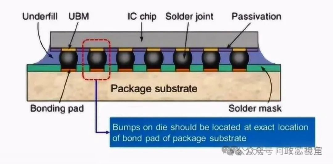
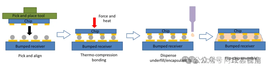
2.1 Process Flow The manufacturing process of flip chips can be simply divided into bump preparation, chip assembly, and underfilling three steps.
 Compared to traditional wire bonding technology, the advantages of flip chip bonding include:① Achieving area array distribution through redistribution layer (RDL), resulting in higher I/O density per unit area;② Shorter interconnection paths, better signal integrity and frequency characteristics;③ Flip chips do not have encapsulation, allowing for effective cooling using heat sinks on the back of the chip, improving heat dissipation capabilities.
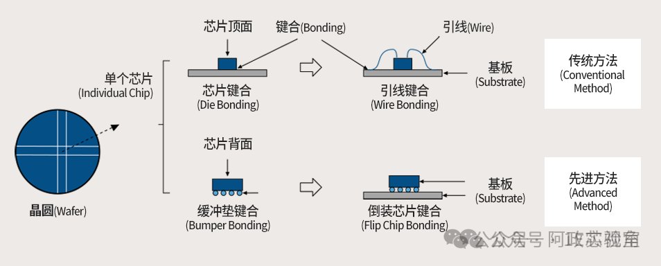 The basic flip chip often uses reflow soldering as the bonding solution (the peak reflow temperature is generally controlled between 240ºC and 260ºC), and a reflow oven can accommodate many processing products simultaneously, so the overall throughput is still very high.However, since the entire chip package is placed in the reflow oven, the chip, substrate, and solder balls expand at different rates, causing warping that prevents the chip from being well bonded, and the molten solder may diffuse beyond its designated area, causing unnecessary electrical connections between adjacent pads and resulting in reduced chip yield.
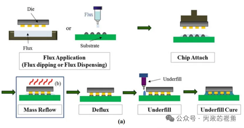
(Common reflow soldering chip bonding process)
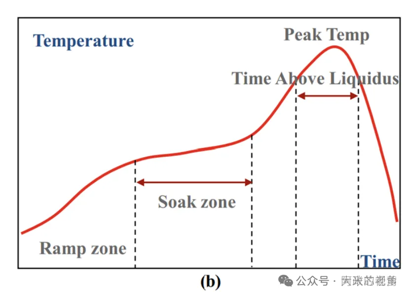
(Common reflow soldering temperature control)
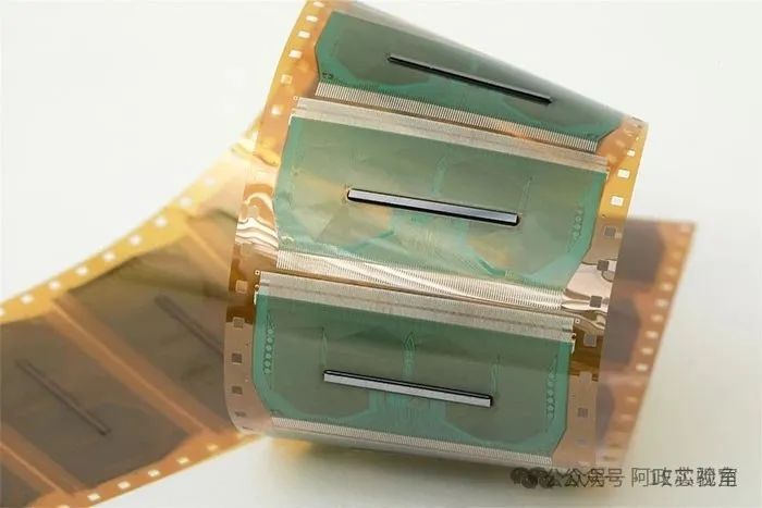
03 Tape Automated Bonding (TAB)
Tape Automated Bonding (TAB) is a chip packaging bonding technology that assembles chips onto flexible tape. The tape serves both as a support for the chip and as the lead for connecting the chip to the external circuit.TAB technology is also known as tape automated soldering or roll tape automated joining.
 3.1 Process Flow
The TAB technology process mainly includes carrier tape production, chip bonding, and packaging protection three stages.
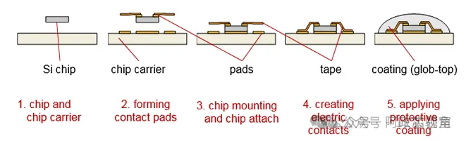
First, the carrier tape is produced by adhering copper foil to polyimide tape, forming fine conductive patterns through photolithography and etching, and creating positioning holes and lead windows; then it enters the inner lead bonding (ILB) stage, where the pre-formed solder bumps are accurately positioned, and all inner leads are connected to the chip pads using thermo-compression or thermo-sonic methods; next, the outer lead bonding (OLB) stage aligns the TAB component with the substrate or PCB, usually using thermo-compression for mass bonding; finally, adhesive or molding protection is applied in the chip area, curing to form a protective layer to enhance reliability.
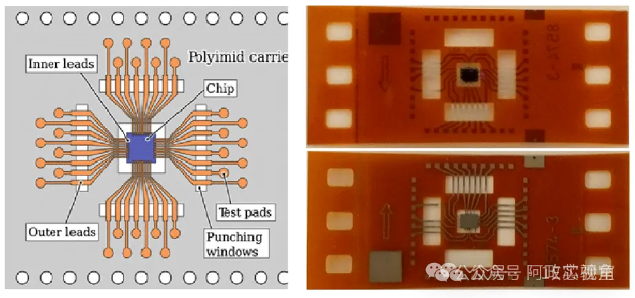
In TAB technology, if only inner lead connections between the chip and the tape are made without outer lead bonding, this application is referred to as TCP (Tape Carrier Package) or COF (Chip On Film) technology, commonly used for packaging display panel driver chips.
TCP/COF packaging
Wire bonding and TAB have similar structures, with the difference being that in wire bonding, the chip’s carrier is a lead frame or PCB substrate, while TAB uses flexible tape; wire bonding uses metal wires for connections, while TAB uses copper foil; in wire bonding, the metal wire is directly soldered to the chip pad, while in TAB, solder bumps are made first before connecting to the copper foil; wire bonding connects one metal wire at a time, while TAB uses prefabricated tape for a one-time connection.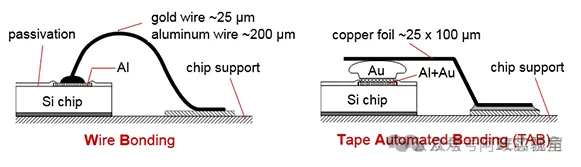
TAB technology’s advantages include suitability for high-density, fine-pitch packaging requirements, enabling mass automated production, and excellent electrical performance (short conductors, low inductance) and heat dissipation, particularly suitable for high-density lead connections such as LCD drivers.
The main disadvantages of TAB technology are high initial investment (requiring customized photolithography masks and specialized equipment), high process requirements (strict alignment accuracy), significant reliability risks due to material thermal expansion coefficient mismatch, and difficulty in maintenance. Additionally, due to high customization, flexibility is limited, making it primarily applicable to specific products in large-scale production.
04 Hybrid Bonding
Both flip chip bonding and thermo-compression bonding use some solder bumps as interconnections between silicon and the packaging substrate, but the bump spacing is physically limited and cannot meet the extremely high interconnection density required for 3D memory stacks and heterogeneous integration. Therefore, hybrid bonding technology was developed.
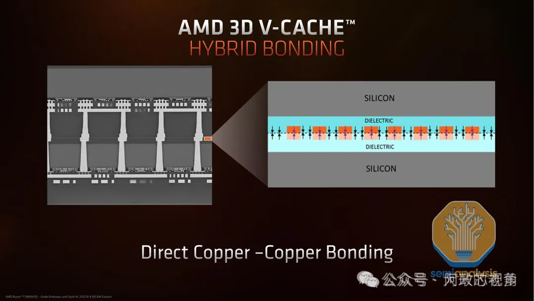
Hybrid bonding is a new type of three-dimensional integrated packaging technology that simultaneously achieves metal bonding (Cu-Cu) and dielectric bonding (oxide-oxide), enabling direct physical and electrical connections at the wafer or chip level. In simple terms, it allows two wafers to be directly connected or chips to be directly packaged onto a wafer. This technology eliminates the need for traditional copper pillars or solder balls, achieving ultra-fine interconnection spacing (<1μm) with extremely high interconnection density. The bonding interface has good flatness, allowing for thinner wafer stacking, which is beneficial for 3D integration. Currently, HBM3 commonly uses thermo-compression bonding technology, and major Korean manufacturers are expected to introduce hybrid bonding starting from HBM4.
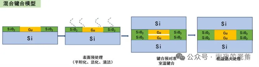
Typical Cu/SiO2 hybrid bonding mainly includes three key process steps.
(1) Pre-bonding treatment: The wafers must undergo chemical mechanical polishing (CMP) and surface activation and cleaning to achieve a flat, clean, and hydrophilic surface;
(2) Pre-alignment bonding of two wafers: Before bonding, the two wafers are pre-aligned and closely adhered at room temperature, allowing the suspended bonds on the dielectric SiO2 to bridge between the wafers, forming a fused bond between SiO2 -SiO2. At this point, there is physical contact or a recessed gap (dishing) between the metal Cu contacts, and complete metal inter-bonding has not been achieved;
(3) Post-bonding thermal annealing: Subsequent thermal annealing promotes the reaction of the dielectric SiO2 between the wafers and the mutual diffusion of the metal Cu, forming a permanent bond.
◎ Advantages: ① Higher I/O density: Compared to micro-bump technology, hybrid bonding can achieve interconnection densities that are 10,000 times higher per unit area, significantly enhancing the connection capability between chips, enabling faster signal transmission with lower power consumption.② Good heat dissipation and mechanical strength, particularly suitable for high-performance computing and memory applications.③ Lower inductance, capacitance, and resistance: The reduced interconnection size in hybrid bonding leads to lower inductance, capacitance, and resistance, enabling faster signal transmission, lower power consumption, and higher overall performance.④ Scalability: Hybrid bonding can be scaled to sub-micron spacing, allowing for finer and more precise interconnections. Research indicates that spacing can be as small as 0.4 microns, with future spacing potentially even smaller. ⑤Streamlined manufacturing process: Compared to micro-bump methods, switching to hybrid bonding interconnections in high bandwidth memory requires fewer process steps, saving costs and improving efficiency. This process involves about 11 steps, resulting in a more streamlined and efficient production. ⑥Flexibility for system architects: Hybrid bonding provides greater creative freedom for system architects when designing chips and systems, facilitating the integration of heterogeneous components and enabling system construction on a chip. This flexibility allows for customization and optimization of systems based on specific requirements.
◎ Disadvantages:This technology has very high requirements for surface cleanliness and flatness, necessitating precise CMP processes and strict surface treatments; it requires stringent cleanliness control of the processing environment, including temperature and humidity; high alignment accuracy is required during the bonding process, leading to high equipment investment costs; the process window is narrow, making yield control challenging; strict requirements for wafer warping and difficulty in rework; additionally, as an emerging technology, the supporting industrial chain is not yet fully developed, the standardization of processes needs further improvement, and reliability data accumulation requires time for validation.
05 Conclusion
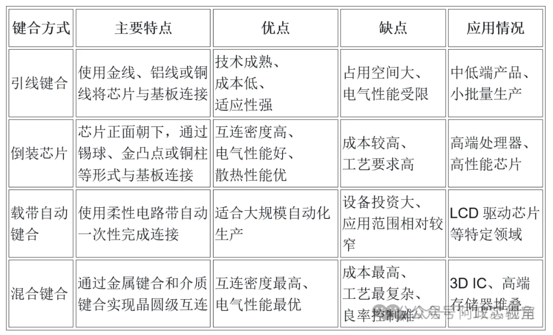
Wire bonding is the most traditional and widely used technology, achieving interconnection between chips and substrates through point-to-point metal wire connections, with mature and reliable processes but lower efficiency.
Flip chip technology connects chips to substrates through bump arrays, offering higher I/O density and better electrical performance, becoming the mainstream for high-performance packaging.
Tape Automated Bonding technology uses prefabricated leads on tape, enabling mass automated production, primarily applied in specific fields such as LCD drivers.
Hybrid bonding is the latest developed technology, achieving ultra-fine interconnection spacing through direct bonding of metal and dielectric, eliminating the need for traditional bump structures, and holds significant application prospects in 3D IC packaging.


Copyright Statement: The information in this article is owned by the original author and does not represent the views of this platform. It is shared for use, and if there are any copyright or information errors, please contact us for correction or deletion. Thank you!