“
The South Korean government and enterprises have successfully achieved a leading position in semiconductor DRAM technology with a research investment that only accounts for 0.024% of GDP. In just 8 years, South Korea transformed the DRAM technology development cycle from being 4 years behind the US and Japan to surpassing them, with semiconductor exports increasing from 3% in the mid-1980s to 20% in 2024, and the global market share of DRAM jumping from less than 1% in 1984 to over 70% in 2024.
The essence of South Korea’s semiconductor innovation consortium lies in the government strategically building a risk-sharing mechanism, proactively investing to solve the issues of “market failure” and “organizational failure” dilemmas. Faced with the high risks of DRAM technology development, the government took the initiative to bear early investments in basic research and common technology breakthroughs, using a model of “funding successful transitions to investments, and not holding failures accountable” to alleviate corporate reluctance and provide ample space for innovation. This “national risk coverage and corporate focus on breakthroughs” collaborative logic enabled South Korea to achieve a qualitative change from following to leading in technology iteration.
With the arrival of the Fourth Industrial Revolution and industrial reshuffling, in recent years, South Korea has further expanded this successful experience to new high-risk technology fields. High-risk new-generation technologies refer to those that may take a long time to commercialize and have a relatively high probability of failure, but once successfully developed, they can directly change the rules of the market. In 2023, the proportion of support for such high-risk technologies in South Korea was only 1% of the budget, but South Korea plans to increase it to 10% by 2028. This initiative reflects the South Korean government’s continued risk-tolerant approach to building a pressure-resistant incubation ecosystem for innovation, promoting strategic industries to achieve a higher level of rise in the Fourth Industrial Revolution and industrial restructuring.
“
Abstract: This article deeply analyzes the key practices and motivations behind the technological breakthroughs achieved by South Korea’s semiconductor industry through the government-industry-academia innovation consortium model from the 1980s to the 1990s. The South Korean government, with strategic foresight, invested only 0.024% of GDP in research funding, successfully promoted DRAM technology from lagging to leading, increasing the proportion of semiconductor exports from 3% in the mid-1980s to 20% in 2024, and the global market share of DRAM jumping from less than 1% in 1984 to over 70% in 2024. Research findings indicate that the core of the South Korean model lies in the government solving market and organizational failure issues through risk-sharing mechanisms, providing strong support for industrial rise. This experience is of great reference significance for promoting the development of other strategic emerging industries.
Keywords:South Korea semiconductor industry; government-industry-academia innovation consortium; DRAM technology; technological breakthroughs; industrial rise
1. Introduction

The semiconductor industry, as a strategic, foundational, and leading industry of modern technology, directly relates to a country’s position in global technological competition. In just a few decades, South Korea has grown from a latecomer in the semiconductor field to a significant global player, with its government-industry-academia innovation consortium model playing a key role. Especially in the breakthrough of DRAM core technology, South Korea has achieved rapid technological catch-up and industrial leap through government strategic planning, resource allocation, and close cooperation between enterprises and research institutions. In 2024, South Korea’s semiconductor export value is expected to reach 141.9 billion USD, accounting for about 20% of total exports, far exceeding traditional advantageous products such as automobiles, ships, petrochemicals, and communication equipment, becoming the core engine of export growth. The global market share of DRAM chips has also exceeded 70%, providing strong momentum for South Korea’s economic growth.This article focuses on the government-industry-academia innovation consortium model during the technological breakthrough phase of South Korea’s semiconductor industry, analyzing its key practices and driving factors, providing valuable references for other regions to promote innovation consortium construction in key areas.
2. The Origin of South Korea’s Semiconductor Innovation Consortium
1. Three Key Motivations for the Formation of South Korea’s Semiconductor Innovation Consortium
1. Government’s Strategic Vision. The South Korean government recognized the critical role of the semiconductor industry in national economic development and technological competitiveness, and decided to vigorously support the development of the semiconductor industry by concentrating efforts through government-industry-academia cooperation to break through technological bottlenecks.
2. Market Demand and Opportunities. With the rapid development of the global semiconductor market, South Korea recognized the enormous potential and importance of the semiconductor industry, while the semiconductor trade conflict between the US and Japan at that time also provided market opportunities for South Korea.
3. Industry Start and Technological Dilemma. In the 1970s, South Korea’s semiconductor industry was in its infancy, lacking independent technology and overly reliant on foreign suppliers, primarily becoming a simple assembly base for transistors and integrated circuits.
2. The Operational Model of South Korea’s Semiconductor Innovation Consortium
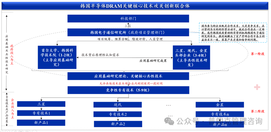
Figure 2.1 South Korea’s Government-Industry-Academia Innovation Consortium Operational Model
3. The Development History of South Korea’s Semiconductor Innovation Consortium’s Key Breakthroughs
1. Early Exploration Stage (1970s – Early 1980s)
The South Korean government launched a semiconductor industry revitalization plan, investing heavily in industry support and research subsidies, promoting domestic enterprises to cooperate with universities and research institutions, and initially establishing a framework for government-industry-academia cooperation.
2. Technological Breakthrough Stage (1980s – 1990s)
Under the leadership of the government, the Korea Electronics and Telecommunications Research Institute led a joint effort with companies such as Samsung, LG, and Hyundai, as well as several universities, to tackle key core technologies such as DRAM, successfully developing and mass-producing a series of 64K, 256K, 1M, and 4M DRAM products, gradually mastering the relevant core technologies and securing a place in the global market.
3. Sustained Development Stage (2000 – Present)
The South Korean semiconductor industry continues to consolidate its advantages, increasing R&D investment in DRAM and flash memory, maintaining a leading technological position. At the same time, it actively expands into emerging fields such as system semiconductors, building a more complete and robust semiconductor industry ecosystem, with the government-industry-academia innovation consortium model continuously deepening and improving.
4. Key Practices and Core Motivations of South Korea’s Government-Industry-Academia Innovation Consortium in Tackling Key Core Technologies (Focusing on DRAM)
In the joint efforts to tackle key core technologies of DRAM, South Korea has built an efficient semiconductor joint organization model, collaborating at three levels: decision-making, management, and execution, ensuring the smooth progress of the tackling work. The following are the key practices and core motivations at each level.
1. Decision-Making Level: Government-Led Strategic Planning and Resource Allocation
1. Government’s Proactive Involvement: Defining Industry Goals and Directions
Key Practice: The South Korean government, based on a precise grasp of global semiconductor market trends and a deep understanding of domestic industry development needs, formulated a clear semiconductor industry development strategy, identifying DRAM as a key breakthrough area, guiding the joint tackling efforts. For example, in the early 1980s, the South Korean government proposed a strategic goal to achieve the autonomy of DRAM technology and reach international advanced levels in a short time, which became the action guide for the joint tackling efforts. The government also developed a detailed technology roadmap, clarifying the R&D milestones and technical indicators from 64K, 256K, 1M to 4M DRAM products, ensuring the orderly progress of the tackling work.
Core Motivation: The government possesses multi-channel intelligence prediction and large-scale resource organization capabilities, able to address the unclear future direction of industry development and the lack of coordinated planning in technology R&D, consolidating efforts to avoid resource dispersion and blind technology development, concentrating resources from enterprises and institutions with different innovation depths to tackle key core technologies of DRAM, promoting rapid development of the semiconductor industry.
2. Resource Allocation: Striving to Solve Market Failure and Organizational Failure Issues.
The government allocated a large amount of funds, manpower, and other resources for joint tackling through the establishment of special funds and industrial policy support. For instance, the South Korean government established the “Electronics Industry Revitalization Fund”, providing almost all funding support for the application basic research and common technology stages of DRAM R&D projects, and coordinating human resources between universities, research institutions, and enterprises to ensure that excellent talents from all parties could participate in the joint tackling efforts. The government also shared the R&D costs with enterprises through tax incentives and financial subsidies, encouraging enterprises to increase their investment in the competitive product technology stage of DRAM, enhancing their R&D enthusiasm. According to statistics, the total R&D funding for the 4M DRAM project was 87.9 billion KRW, of which research equipment costs were 47.9 billion, and net research costs were 40 billion. Enterprises bore 57.9 billion KRW (including the industrial technology enhancement fund of 20 billion), while the government contributed 30 billion KRW (with 10 billion from the Science and Technology Department and 20 billion from the Communication Corporation). This accounted for 0.024% of the total GDP at that time (370.68 trillion KRW).
Core Motivation: In the application basic research and common technology research stages, there are significant risks of failure, leading to insufficient willingness of enterprises to invest, which is a market failure issue. At the same time, the semiconductor industry was still an emerging industry, and the research capabilities of South Korean market entities had not yet developed to the point of achieving full-process innovation. The breakthroughs in the key technologies of DRAM involved solving application basic research and competitive product technologies, which could not be resolved by a single university, research institute, or enterprise, leading to organizational failure issues. Additionally, there was a shortage of top talents in emerging industries. The government’s funding entry addressed the issues of insufficient R&D funding, talent shortages, and high risks that led to low enthusiasm for enterprise R&D, providing strong financial and human support for joint tackling, sharing and compensating for enterprise R&D risks and costs, and accelerating the R&D and industrialization process of DRAM technology.
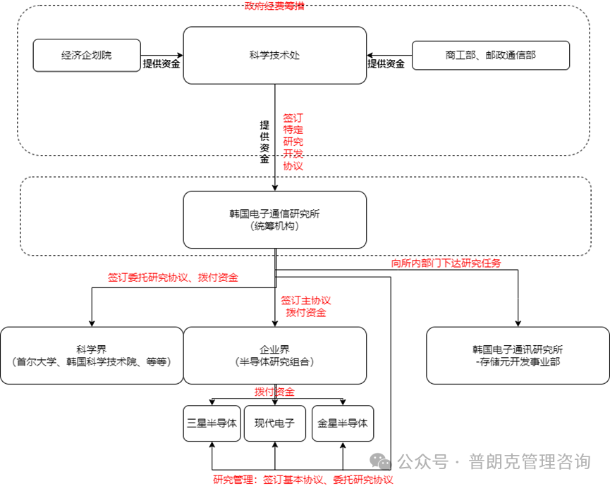
Figure 4.1 Resource Allocation for Joint Tackling Tasks of DRAM
3. Leapfrog R&D Model: Accelerating Technological Catch-Up and Iteration
The development of South Korea’s DRAM technology has followed a clear trajectory from 4M to 16M, 64M, 256M, and then to 1G, with clear and forward-looking R&D goals. However, facing the rapid iteration characteristics of semiconductor technology, traditional gradual R&D models are insufficient to meet the demands for rapid technological advancement and market competitiveness. Therefore, Samsung was the first to abandon the step-by-step R&D path, innovatively adopting a leapfrog R&D model, which played a crucial role in the development of South Korea’s DRAM technology. Specifically, Samsung set up two R&D teams, advancing R&D tasks according to the nodes of “1-3-5” and “2-4-6”. For example, the team that completed the 4M DRAM tackling directly entered the research of 64M, skipping 16M; while the team that completed 16M continued to work on 256M R&D.This leapfrog model breaks the linear thinking of traditional R&D, allowing R&D teams to skip certain intermediate technology stages and directly aim for more advanced technological goals, significantly shortening the time for technology to transition from following to leading.
Core Motivation: This model addresses the issues of long R&D cycles and rapid iteration speeds. The semiconductor industry experiences rapid technological updates, and traditional gradual R&D models may cause enterprises to miss market opportunities during the catch-up process. Through the leapfrog R&D model, South Korea ultimately achieved a leap from technology introduction to independent innovation. This model not only promoted the rapid development of South Korea’s DRAM technology but also provided valuable experience for technological innovation in the global semiconductor industry.
4. “Funding Transition to Investment”: Building a Funding Cycle and Sustainable Development Model
The 4M DRAM project belongs to the “specific research and development project” that clearly stipulates that the patent ownership obtained during the project R&D process is shared between the government and enterprises. Thanks to the government’s early research investments and organization, and the substantial financial support provided to enterprises, participating companies have gained significant benefits at the product end, widely recognizing and agreeing to pay the government technology usage fees, forming a “corporate feedback and funding transition to investment” funding cycle model, promoting continuous development in the technology field, while also allowing the government to grasp the landing and profitability of joint R&D project results, providing a basis for policy effect evaluation and improvement.
Core Motivation: This model addresses the sustainability of government R&D funding. Through the success of projects, enterprises paying technology usage fees form a funding cycle, ensuring that the government can continuously support more research projects. At the same time, through patent sharing and funding recovery mechanisms, the government can grasp the marketization of project results, providing data support for policy evaluation and improvement, optimizing resource allocation, and enhancing the scientificity and effectiveness of policies.
2. Management Level: Coordination and Management by Leading Institutions
1. Interest Coordination: Balancing Demands from All Parties to Enhance Cooperation Efficiency
The Korea Electronics and Telecommunications Research Institute, as the leading unit, plays a crucial role in coordinating the interests of all parties at the management level. During the joint tackling process, different enterprises, universities, and research institutions have their own interest demands. The leading institution balances these interests by establishing reasonable benefit distribution mechanisms and encouraging competitive strategies, ensuring that all parties can actively engage in the tackling work. For example, in the distribution of intellectual property rights from R&D results, the leading institution has established fair and reasonable rules, clarifying the rights and interests of all parties, avoiding delays in tackling progress due to disputes over interests. The leading institution also formulates corresponding reward mechanisms based on the contributions of each party in the tackling process, providing material and spiritual rewards to units and individuals that perform outstandingly in the tackling efforts, enhancing participation enthusiasm from all parties.
Core Motivation: Since participating enterprises are both collaborators and competitors, there are certain difficulties in cooperation in profit-oriented business activities. Choosing the non-profit organization Korea Electronics and Telecommunications Research Institute as the leading unit effectively resolves the inconsistencies in interest demands among government, industry, and academia, which can easily lead to conflicts and disputes. The allocation of R&D resources, represented by the disbursement of R&D funds, is seen as the primary means of restraint and incentive for participating entities, ensuring that all parties can form a joint force in the tackling of DRAM technology, improving tackling efficiency and result quality.
2. Task Allocation and Supervision: Precisely Configuring Resources to Ensure Progress in Tackling
The leading institution reasonably allocates joint tackling tasks based on the advantages and characteristics of each unit and supervises the execution of tasks. In the DRAM tackling project, the leading institution assigned basic research tasks to universities and research institutions, while mainly assigning process R&D and product development tasks to enterprises, and established 3-4 milestone nodes to check and evaluate the execution of tasks, ensuring that each task can be carried out in an orderly manner according to plan, improving the overall efficiency and quality of the tackling work. For example, in the process of enterprise technology R&D, a phased guidance strategy is adopted for different technology types. For the joint R&D of core common technologies, emphasis is always placed on guiding information exchange and result sharing among enterprises. For the shared R&D of individual common technologies, from the second year onwards, R&D topics and funding are tilted towards enterprises with stronger R&D capabilities, strengthening the competitive mechanism. For the proprietary competitive technologies developed separately, the first year focuses on guiding enterprises to achieve independent control of the technologies required for storage cell design and product development; the second year emphasizes guiding enterprises to formulate market strategies and differentiate product types, and to carry out early R&D of next-generation technologies; the third year further guides enterprises to improve models and conduct R&D for mass production technologies.
Core Motivation: This mechanism addresses the issues of unreasonable task allocation in technology R&D and the lack of effective supervision of R&D work, which can lead to delays in tackling progress and substandard quality. The task allocation and supervision mechanism’s core motivation is to systematically solve the fragmentation, low efficiency, and high-risk issues in DRAM R&D through resource integration of research entities, full-chain collaboration, phased control, and balancing competition and cooperation, ultimately achieving the dual goals of technological independence and market competitiveness.
3. Communication Coordination: Promoting Information Sharing to Address Collaborative Shortcomings
The leading institution is also responsible for establishing an efficient communication coordination mechanism to promote information sharing and exchange among units. During the tackling process, the leading institution regularly organizes project meetings, allowing each participating unit to report on work progress, exchange technical difficulties and solutions, and promptly resolve issues encountered during the R&D process, strengthening collaboration among units. For example, the leading institution organizes a project progress report meeting every month, where each participating unit reports in detail on task progress, encountered problems, and next steps. The leading institution coordinates to resolve common issues such as resource shortages and technical difficulties based on the reports from each unit, and promptly adjusts the tackling plans and task allocations to ensure the smooth progress of the tackling work. The leading institution has also established a project information sharing platform, where units can upload technical materials, experimental data, etc., from the R&D process for other units to reference, promoting knowledge sharing and technical exchange.
Core Motivation: This mechanism addresses the issues of low R&D efficiency and repetitive work caused by poor communication and untimely communication among units in government-industry-academia cooperation, promoting collaboration among units, accelerating the R&D process of DRAM technology, and improving innovation efficiency.
4. Intelligence Monitoring Model: Ensuring R&D Direction is in Sync with International Frontiers
Monitoring and analyzing intelligence throughout the process is a crucial part of managing the core key technologies tackled by South Korea’s DRAM research team. Throughout the project, technology trend investigations are conducted, monitoring the technological levels, main research technology routes, core research teams, advantages and disadvantages of technologies in various countries, and future applications in real-time. Before project initiation, international technology trend investigations are important materials for project applications, requiring a focus on explaining the current state of technology development and the necessity of project initiation; during project implementation, real-time monitoring of the latest international technological developments is conducted, and when significant changes occur in the external environment and technology, dynamic target strategies are adopted to adjust the technological direction and route in a timely manner to avoid redundant research or straying further down the wrong path; at the conclusion stage, similar investigations into international technology trends are conducted to evaluate project results and determine their position in the global technological landscape.
Core Motivation: This model addresses the issues of information asymmetry and deviations in technological direction during the R&D process, ensuring the correctness of the R&D direction and the advancement of the technological route through comprehensive intelligence monitoring, avoiding resource waste and R&D risks.
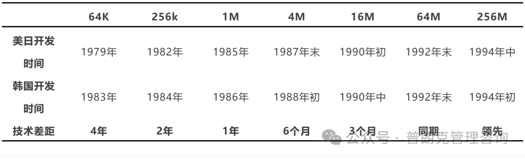
Table 4-1 Comparison of DRAM Technology Levels Between South Korea and the US/Japan
5. Talent Introduction Model: Combining External Breakthroughs with Independent Cultivation
Innovation is the primary driving force for development, and talent is the first resource for innovation, especially in core technology fields. In the face of technological blockades from advanced countries like the US and Japan, South Korea has turned its attention to high-end talents of Korean descent and international students in the DRAM field, attracting a large number of talents back to South Korea with the prospects of future development and patriotic sentiments. The return of these talents has not only laid the foundation for the leapfrog development of South Korea’s DRAM but has also played an important role in enhancing the technical level of domestic researchers and cultivating talents.
Core Motivation: In the face of key technology acquisition dilemmas caused by technological blockades from the US and Japan and a shortage of high-end local talents, South Korea has quickly filled technological gaps and broken external blockades by attracting Korean experts and international students, also promoting the growth of local research teams, forming a “introduction—breakthrough—cultivation” virtuous cycle, ultimately achieving independent leapfrog development of DRAM technology.
3. Execution Level: Collaborative Technology R&D and Innovation
1. Basic Theoretical Achievements: Laying a Solid Technological Foundation to Drive Innovative Leapfrogging
Universities and research institutions at the execution level are mainly responsible for conducting basic theoretical research and technological frontier exploration of DRAM, providing theoretical support and technical reserves for enterprises’ technological R&D. For example, South Korean universities such as KAIST (Korea Advanced Institute of Science and Technology) conduct in-depth research in foundational fields such as semiconductor physics and materials science, achieving a series of important results that provide a solid theoretical foundation for enterprises to tackle key core technology challenges in DRAM. Universities and research institutions also actively engage in international exchanges and cooperation, establishing partnerships with renowned foreign universities and research institutions, introducing advanced research methods and technologies from abroad, enhancing South Korea’s level in the foundational research field of DRAM. For instance, Sungkyunkwan University in South Korea has established a joint research center with Stanford University in the US, collaborating on research projects in the foundational research of DRAM, exchanging academic results, and cultivating a batch of semiconductor foundational research talents with international perspectives in South Korea. These basic theoretical research achievements not only deepen the understanding of the working principles and performance limits of DRAM, but also provide important theoretical basis for subsequent process R&D and product innovation, such as theoretical breakthroughs in storage cell structure optimization and the application of new semiconductor materials, laying the foundation for improving key performance indicators such as storage density and reducing power consumption of DRAM.
Core Motivation: This model addresses the weaknesses in South Korea’s foundational research in DRAM, lacking independent intellectual property rights and international competitiveness, providing solid theoretical support and cutting-edge technology reserves for DRAM technology R&D, promoting the transformation of South Korea’s semiconductor industry from technology following to technology innovation.
2. Joint Collaboration: Overcoming Common Technologies at the Bottom Level to Achieve Independent Control
In terms of common technologies at the bottom level, guiding participating enterprises in interaction, communication, and mutual application of results during the R&D process, the joint tackling team concentrated efforts to overcome key common technology challenges in the manufacturing process of DRAM, providing strong support for the large-scale production and performance enhancement of DRAM products. For example, in photolithography technology, through government-industry-academia cooperation, South Korea successfully developed high-precision photolithography processes, achieving smaller sizes of DRAM chip manufacturing, improving chip integration and performance. At the same time, significant breakthroughs have also been made in key manufacturing technologies such as thin film deposition and doping processes, ensuring high-quality production of DRAM chips. Additionally, the joint tackling team conducted in-depth research on storage capacitor technology for DRAM, developing high-performance storage capacitor structures and materials, effectively enhancing the data storage capacity and reliability of DRAM. These breakthroughs in common technologies not only reduced R&D costs and risks for enterprises but also accelerated the iteration of DRAM technology, allowing South Korea’s semiconductor industry to gradually break free from dependence on foreign technologies and achieve independent control.
Core Motivation: This model addresses the issues of key common technologies in the manufacturing process of DRAM being constrained by external factors, high production costs, and unstable product quality, guiding participating enterprises in interaction and communication during the R&D process, accelerating the diffusion of common technologies, sharing R&D costs and risks, and enhancing South Korea’s semiconductor industry’s independent control capabilities and market competitiveness in the DRAM manufacturing field.
Column 1: Execution of Key Core Common Technologies
|
Technology Type: Key Core Technology Technology Content: Protective film and packaging technology, simulation technology, detection and reliability technology R&D Method: Joint R&D, collaborating on different links of the same core key common technology in a common production area, with participating enterprises dispatching resident personnel. Disbursement Rules: Equal disbursement of R&D funds to three enterprises from start to finish. |
Column 2: Execution of Common Technology Groups
|
Technology Type: Common Technology Group Technology Content: Micro-line width etching technology, component isolation technology, thin film dielectric formation technology, wiring technology, three-dimensional structure capacitor technology R&D Method: Based on common technology categories, sharing R&D tasks, with participating enterprises sending researchers to participate. Disbursement Rules: Initial differential disbursement to avoid the “free-rider effect”; equal disbursement of 60% of the first phase budget before the first evaluation; after the first evaluation, the first and second-ranked enterprises receive 75% of the second phase budget, while the third-ranked enterprise receives 60%; after the second evaluation, the first and second-ranked enterprises receive equal disbursement, while the third-ranked enterprise’s disbursement is interrupted, but it still needs to complete tasks and self-fund; after the third year, equal payment is made to all participating enterprises after settling R&D performance and funding expenditures. |
3. Competitive (Proprietary) Technology Tackling Model: Multiple Routes of Competition to Accelerate Technological Breakthroughs
South Korea’s DRAM technology tackling adopts a competitive model of common technology joint development and multiple routes of competitive proprietary technology research simultaneously. For common technologies, a certain range of technology and knowledge sharing is achieved; for key core proprietary technologies such as production technology and process technology, participating institutions independently develop and introduce competition models. At that time, the mainstream DRAM process technology routes had two types: trench and stacked. Faced with this situation, South Korean enterprises each chose a technology route for tackling, with Samsung adopting the stacked method and achieving success first; LG then adopted a hybrid method, completing second; and Hyundai initially adopting the trench method before switching to the stacked method. Internally, a competitive model was also introduced, for example, Samsung divided its R&D teams into domestic and overseas groups to jointly research a technology, accelerating the speed of tackling key core technologies, allowing almost all DRAM technology breakthroughs in South Korea to occur ahead of schedule.
Core Motivation: This model addresses the uncertainties in technology route selection and stimulates corporate innovation vitality through competition among multiple technology routes and evaluations at multiple milestone stages, accelerating key technological breakthroughs, reducing the risks of technology selection errors, while promoting healthy competition and cooperation among enterprises, enhancing overall R&D efficiency and result quality.
Column 3: Execution of Competitive (Proprietary) Technologies
|
Technology Type: Competitive (Proprietary) Technology Technology Content: Product design technology, integrated process technology, component technology R&D Method: Independent development, with process management advancing according to the strategy of “first achieving technological independence and control, then determining basic product models, and finally optimizing models.” Disbursement Rules: R&D funding is supported according to the method of “first equal disbursement, then preferential resource allocation”: R&D funding disbursement is linked to evaluation results, with the three enterprises having the same evaluation time and standards. Before the third evaluation, funds are equally disbursed; after the first and second evaluations, the first-ranked enterprise receives an additional 900 million KRW; during the third and fourth evaluations, the second and third-ranked enterprises must pay 600 million KRW to the first-ranked enterprise. |
4. Product Development: Government Solving Front-End Problems, Enterprises Focusing on Development
Enterprises play a leading role at the execution level, responsible for transforming and applying the basic research results and common technologies from universities and research institutions, conducting DRAM process R&D and product development.The South Korean government actively addresses high-risk technology issues at the front end, paving the way for enterprise development through the government-industry-academia cooperation model, concentrating efforts to tackle key common technologies in DRAM manufacturing. For example, breakthroughs have been achieved in key technologies such as photolithography and thin film deposition, reducing the R&D risks and costs for enterprises. This has made profit-oriented enterprises enthusiastic during the product development phase, allowing them to focus more on transforming technological achievements into actual products. According to the Korea Institute for Industrial Economics and Technology (KIET), between 1980 and 2000, every 1 KRW invested in R&D in the semiconductor industry generated about 83 KRW in added value. The proportion of semiconductor exports increased from 3% in the mid-1980s to 20% in 2024; the global market share of DRAM jumped from less than 1% in 1984 to over 70% in 2024.
Enterprises such as Samsung, LG, and Hyundai play a leading role at the execution level, transforming the basic research results and common technologies from universities and research institutions into actual products. These enterprises invest heavily in DRAM R&D, achieving significant breakthroughs in chip design and manufacturing process improvements, successfully developing a series of 64K, 256K, 1M, and 4M DRAM products, gradually narrowing the gap with international advanced levels and achieving breakthroughs in certain technologies.
For example, Samsung Electronics developed the 64K DRAM in 1983 and achieved mass production in 1984, subsequently launching higher-capacity DRAM products, significantly enhancing South Korea’s competitiveness in the global semiconductor market. Enterprises also focus on optimizing product performance based on market demand and customer feedback, expanding market channels, and strengthening brand building, driving products into the global market, enhancing the market share and brand awareness of South Korea’s semiconductor industry. Samsung Electronics’ semiconductor division achieved revenues of 63.6 billion USD in 2023, accounting for 28% of the group’s total revenue.
Core Motivation: The South Korean semiconductor industry once faced issues of lacking independent products and weak market competitiveness. The government, by addressing high-risk technology issues at the front end, lowered the technical thresholds and risks for enterprises’ R&D, stimulating enthusiasm for product development. Enterprise-led product development transforms research achievements into actual products, meeting market demands, enhancing the global market share and competitiveness of South Korea’s DRAM products, achieving rapid industrial development and economic benefit growth.
5. Conclusion
From the 1980s to the 1990s, South Korea’s government-industry-academia innovation consortium model achieved remarkable results in tackling key core technologies of DRAM, providing strong support for the rise of South Korea’s semiconductor industry. This model effectively addresses key issues in industrial development, such as unclear direction, insufficient resources, conflicts of interest, and technological bottlenecks through the collaboration of decision-making, management, and execution levels. Its successful experience is not only applicable to the semiconductor field but also provides valuable references for the development of other strategic emerging industries.
Conclusion: The essence of the innovation consortium lies in the government strategically building a risk-sharing mechanism, resolving corporate reluctance through “funding successful transitions to investments, and not holding failures accountable”, breaking through the dilemmas of “market failure” and “organizational failure”.
Recommended Related Reading:
-
The Origin, Stages, Key Practices, and Motivations of the US Defense Advanced Research Projects Agency (DARPA)
-
The Origin, Development, Key Practices, and Motivations of the Fraunhofer Society in Germany
-
The Origin, Stages, Key Practices, and Motivations of Israeli Incubators
-
What Can I Bring You?
Thank you for your attention~ Because of your sharing, our knowledge has gained another layer of meaning and value

Planck Management Consulting
Planckist
“All things grow together without harming each other” — from the Doctrine of the Mean

@
Little Assistant: [email protected]
Becoming the Planck of the Technology Policy Research Community