1. Signal Crosstalk
Crosstalk refers to the coupling phenomenon between two signal lines. Due to the close spatial distance, there will be unwanted inductive and capacitive coupling between the signal lines, leading to mutual interference. Capacitive coupling can cause coupling currents, while inductive coupling can cause coupling voltages. This is a tricky issue in circuit design.
2. Overview of This Article
The problem to be solved in this article is the high waveform noise interference at the RS485 transmitter. As shown in Figure 1, the schematic diagram connects the RS485 transmit, receive, and enable control pins directly to the MCU port through a 10R resistor. This circuit is a commonly used RS485 solution on the market, and the specific implementation method is as follows:
During idle periods, 485EN is low, and the MCU is in receive mode; before preparing to send data, the MCU will pull 485EN high, and U25 is in transmit mode; after sending is complete, 485EN returns to low, and U25 is in receive mode. The key to this solution is to master the timing of controlling the high and low of the 485EN pin; otherwise, packet loss may occur.
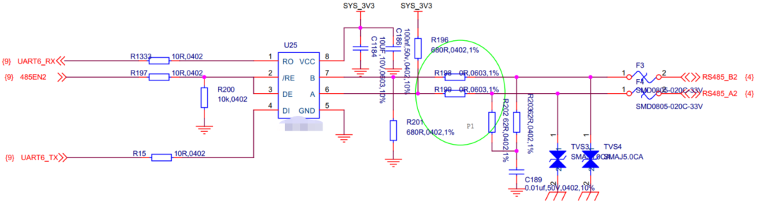
Figure 1: Typical Application Schematic of RS485
3. Problem Discovery and Resolution Process
During hardware testing, it was found that the waveform of the transmitter DI was as shown in Figure 2, with significant spikes on the signal (the resistance R15 before and after is the same). Measuring another identical RS485 circuit does not show this issue, and analyzing the circuit principle shows no problems, leading to the suspicion that this signal is being interfered with by other signals.
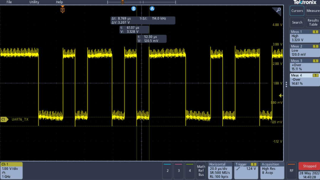
Figure 2: Waveform of RS485 Transmitter Pin DI (UART6_TX)
Opening the PCB diagram, we find the PCB routing corresponding to the UART6_TX line, as shown in Figures 3 and 4. We can see that this line comes out from the MCU through a via to the third layer, then goes straight up, returning to the first layer through another via, and then connects to the DI pin of the RS485 chip through the R15 resistor. Apart from a short distance of parallel wiring with the DCDC_OUT line on the first layer, the rest is relatively clean. Checking the DCDC_OUT signal, we find that DCDC_OUT is the core voltage of the MCU, and the selected MCU contains a PMU unit with the internal DCDC unit being part of it, as shown in the block diagram in Figure 5. Considering the strong interference from the buck chip, it is suspected that the core DCDC output wiring is causing coupling interference to UART6_TX.
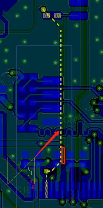
Figure 3: UART6_TX Routing Path
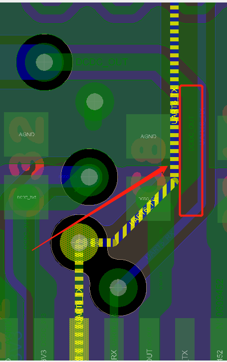
Figure 4: Parallel Wiring Section of UART6_TX and DCDC_OUT
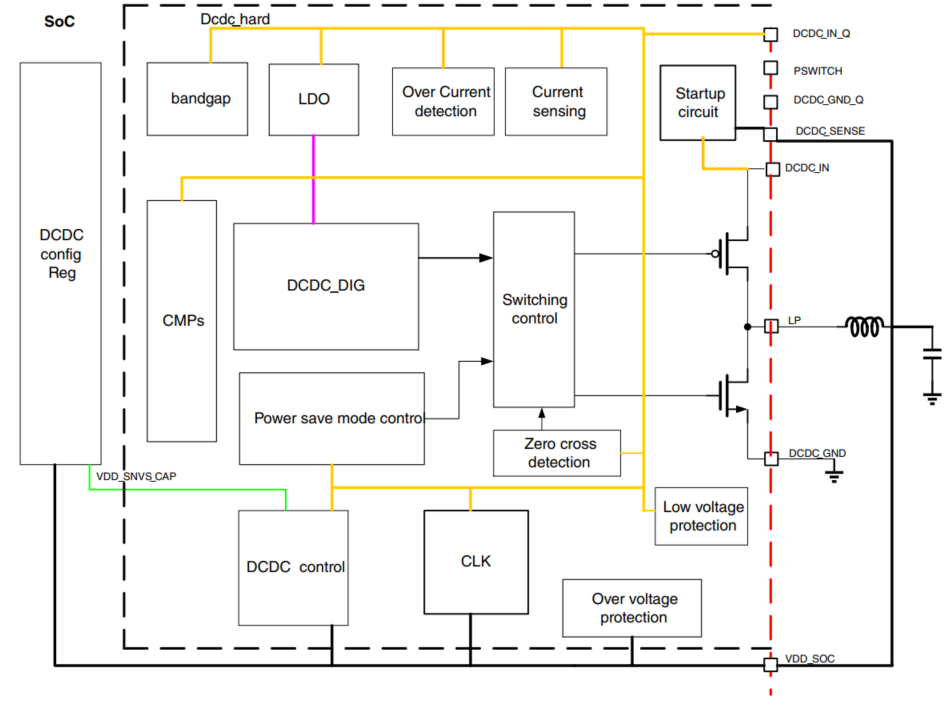
Figure 5: DCDC Block Diagram
Simultaneously monitoring the voltage waveform of the RS485 transmitting pin DI and the LP point (before the inductor in Figure 5), as shown in Figure 6, it can be observed that the frequency of the interference is basically consistent with the frequency at the LP point, which can basically confirm that the coupling interference is coming from the parallel output wiring of the chip core power buck chip to the RS485 DI pin.
Note: Yellow represents the waveform on RS485, LP point waveform
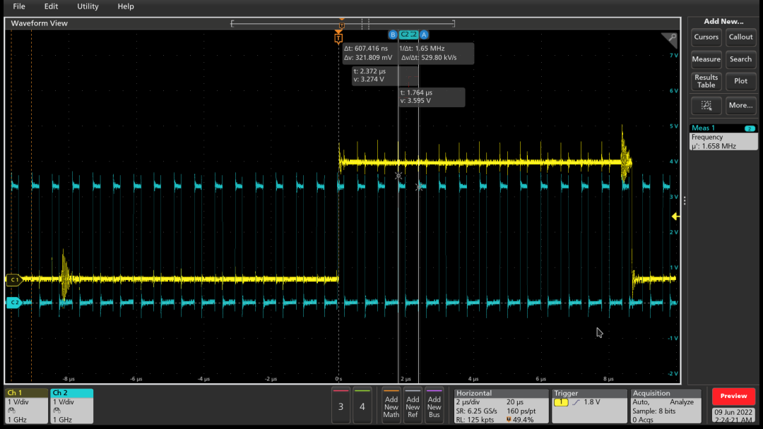
Figure 6: Waveform of Transmitter DI and LP Point
Some might say that this judgment seems a bit hasty. Is it possible that the RS485 chip part is receiving interference from elsewhere before the transmitter? Alright, let’s verify: we first disconnect the R15 resistor and then observe the waveform near the MCU end and the output voltage waveform at the LP point, as shown in Figure 7. It is found that after disconnecting R15, the interference waveform still exists. Measuring the DI pin waveform, as shown in Figure 8, shows no interference. Therefore, it is basically confirmed that the interference comes from the parallel wiring section of DCDC_OUT and UART6_TX.
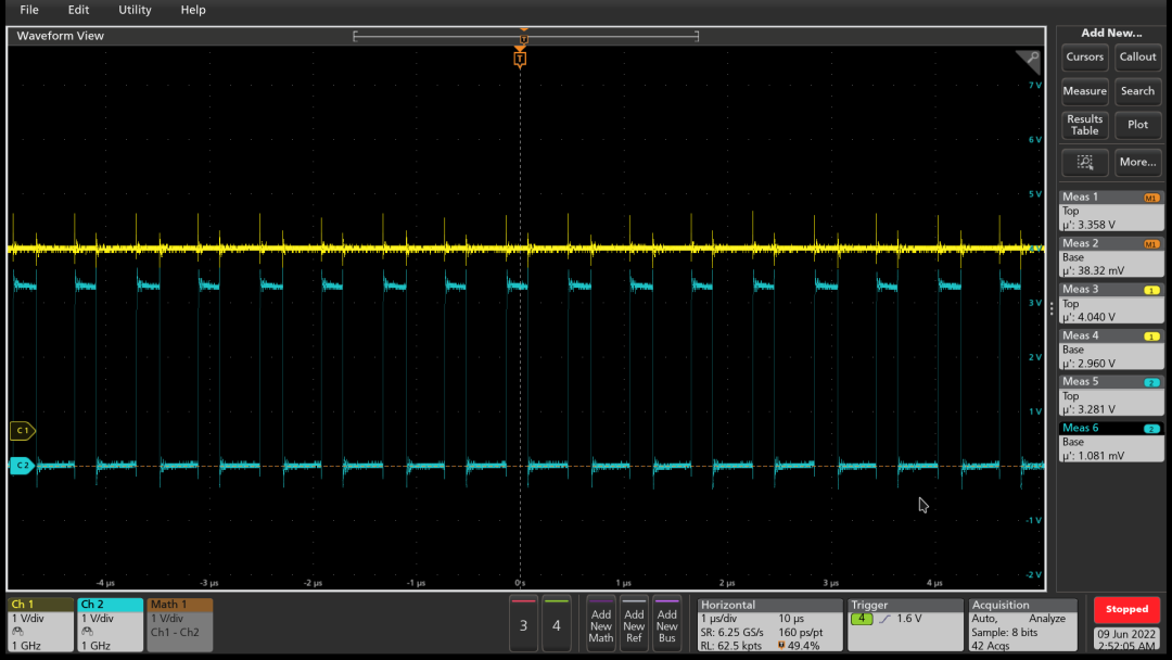
Figure 7: Waveform Measurement of MCU End and LP Point After R15 Disconnection

Figure 8: DI Pin Waveform Measurement After R15 Disconnection (Yellow)
4. Solution
Now that the cause has been found, how to eliminate the interference?
1. When wiring, change this section of parallel wiring to avoid parallel wiring or increase the wiring distance;
2. Add a small capacitor to the RS485 sending DE pin to filter out noise, as the noise frequency is at 1.65MHz, while the maximum RS485 frequency is 110k, which is a large frequency difference, making it easy to filter. Below are the test waveform diagrams when adding capacitors of different values at the DI pin. Considering the need to eliminate interference while ensuring the quality of the signal waveform’s rising and falling edges, a 1nF capacitor is ultimately chosen.
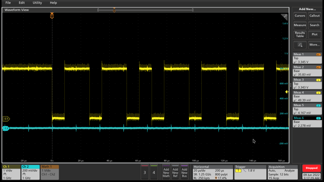
Figure 9: DI Pin Waveform at 22pF
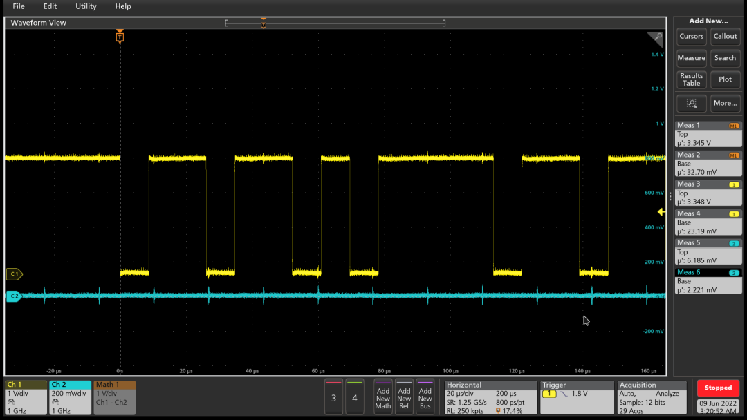
Figure 10: DI Pin Waveform at 220pF
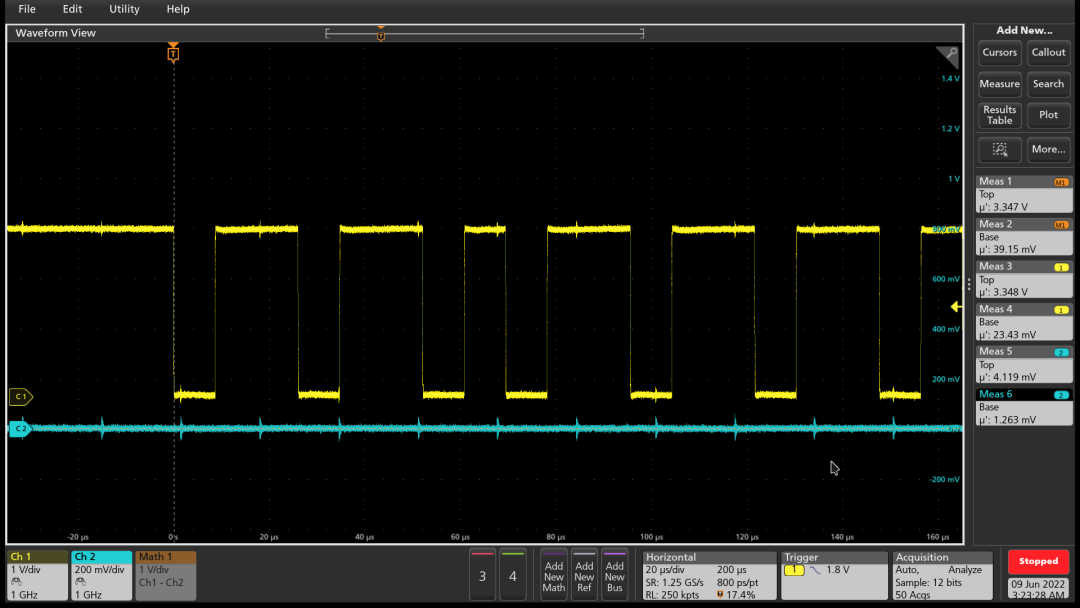
Figure 11: DI Pin Waveform at 1nF
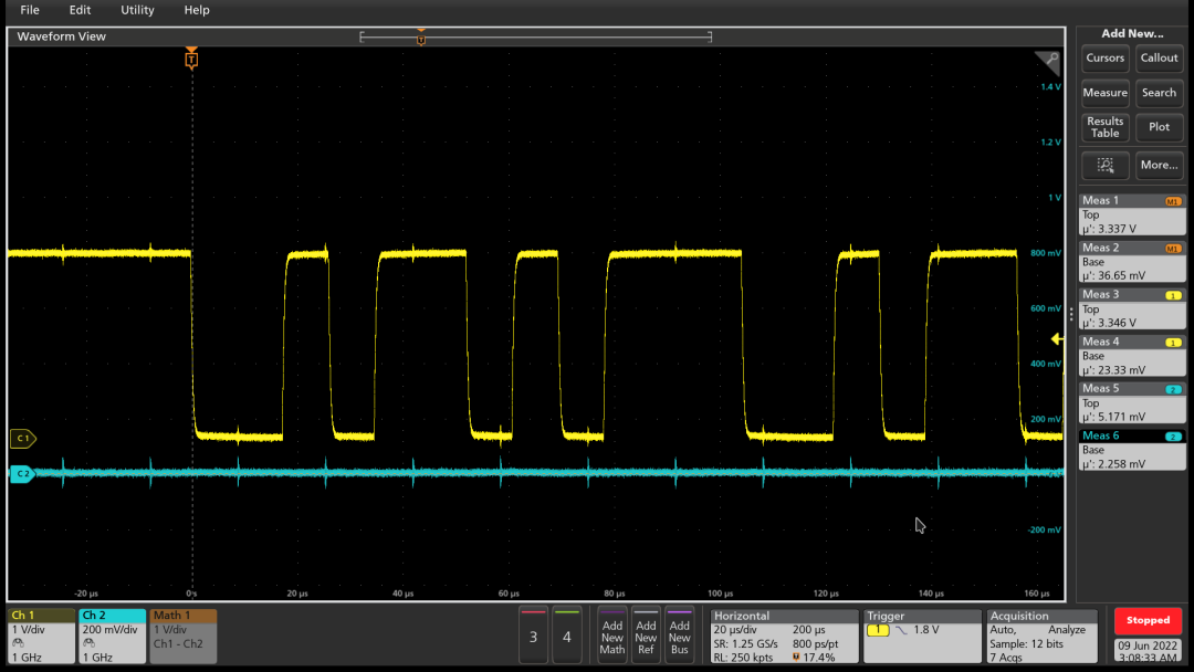
Figure 12: DI Pin Waveform at 10nF

In this issue, we discuss fake chips. What experiences do you have? Rewards for sharing!This issue’s activity theme:Have you been deceived by fake chips or components?You can share content such as:1. Have you encountered counterfeit chips or refurbished materials?2. What troubles did this cause you?3. How did the other party commit fraud?4. How did you identify it?5. Any insights to share?
Activity Prizes:First Prize: 300 Yuan JD E-cardSeveral Excellent Prizes: 50 Yuan JD E-cardParticipation also earns a 20 Yuan JD E-card reward!

Scan to see colleagues’ experiences of being “duped”
