Next, we will analyze it step by step.
1. I2C Start Signal
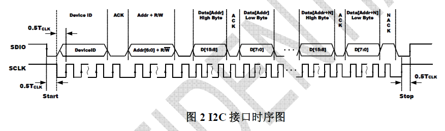
Observe the timing diagram; a falling edge on SDIO while SCLK is high represents the start signal.
void I2C_Start(){ // Set the two pins used for I2C to output mode pinMode(SCLK_PIN, OUTPUT); pinMode(SDIO_PIN, OUTPUT); // When SCL is high, a falling edge on SDA represents the start signal digitalWrite(SDIO_PIN, 1); digitalWrite(SCLK_PIN, 1); digitalWrite(SDIO_PIN, 0);}The above code sets both pins to output mode first, then outputs a falling edge on the SDIO pin while SCLK is high.
2. I2C Stop Signal
Observe the timing diagram; a rising edge on SDIO while SCLK is high represents the stop signal.
void I2C_Stop(){ pinMode(SDIO_PIN, OUTPUT); // When SCL is high, a rising edge on SDA represents the stop signal digitalWrite(SDIO_PIN, 0); digitalWrite(SCLK_PIN, 1); digitalWrite(SDIO_PIN, 1);}This is basic IO operation written in Arduino; you can replace it with any microcontroller’s IO operations.
Since the SCLK pin remains in output mode throughout the process, we only need to initialize SCLK as output during the start signal, while the SDIO pin’s input/output mode may change, so other functions need to set the SDIO pin’s mode as needed.
Three lines of code achieve a rising edge on SDIO while SCLK is high, implementing the stop signal.
3. Write Byte Operation
Next, we will write the operation in a readable manner according to the timing.
Reading and writing bytes in I2C is defined as follows: when the clock line is low, the data line’s level can be modified; when the clock line is high, the data line’s state is read.
Since this is a write operation, we first pull the clock line SCLK low, then modify the value of SDIO, and finally pull the clock high. After pulling high, the slave will read the state of SDIO from the bus, and then send one bit at a time.
void I2C_Write(uint8_t dat){ pinMode(SDIO_PIN, OUTPUT); // After pulling the clock line low, we can modify the data line's state digitalWrite(SCLK_PIN, 0); for(int i=0;i<8;i++) { digitalWrite(SDIO_PIN, (bool)(dat&0x80)); digitalWrite(SCLK_PIN, 1); // Send data when high dat=dat<<1; digitalWrite(SCLK_PIN, 0); // Pull low to prepare for the next bit's sending }}The above code describes this situation: to ensure that the last level is low, the first pull down of SCLK is placed outside the loop, allowing a byte write task to be completed with the least number of execution times; simultaneously, after completing a byte write, the clock line remains low (the first byte written in the timing diagram is DeviceID, the second byte is the register address + read/write bit).
After writing a byte, the slave will send an acknowledgment of the write event, at which point the master can read the acknowledgment signal from the bus.
4. Read Slave Acknowledgment Signal
The acknowledgment signal is sent by the slave after a byte is written, and it can be read while the clock is high. We note that after writing the operation, the clock line is already low, so at this time
we just need to pull the clock line high, and then we can read the acknowledgment signal. After reading the acknowledgment signal, we should pull the clock low to prepare for the next byte’s write.
bool I2C_RACK(){ bool ack; pinMode(SDIO_PIN, INPUT); digitalWrite(SCLK_PIN, 1); // Receive acknowledgment signal; when the clock is high, the slave sends out the acknowledgment signal ack = digitalRead(SDIO_PIN); digitalWrite(SCLK_PIN, 0); // Pull low after reading the acknowledgment signal. return ack;}As shown in the above code, it receives the slave acknowledgment, pulls the clock high, reads the acknowledgment, then pulls low and returns the acknowledgment. If the slave acknowledges, a low level will be read here.
Next, write a register + read/write bit address, referring to the above write operation.
After writing the register address, we immediately receive another acknowledgment signal from the slave, and then the slave will send out data. The sent data consists of high byte and low byte, and there must be a master sending an acknowledgment signal to the slave between the high and low bytes, so that the slave knows the master has received the data, and will send out the subsequent low byte data.
5. Read Byte Operation
Note that as mentioned earlier, both reading and writing modify the data line when the clock is low and send out when the clock is high.
Therefore, the master reads the data sent by the slave while still reading during the high level.
uint8_t I2C_Read(){ uint8_t dat=0; pinMode(SDIO_PIN, INPUT); for(int i=0;i<8;i++) { digitalWrite(SCLK_PIN, 1); // Read data while the clock is high dat=dat<<1; if(digitalRead(SDIO_PIN)) { dat=dat|1; } digitalWrite(SCLK_PIN, 0); // Pull low to prepare for the next bit's reading } return dat;}The operation process sets the SDIO data line’s IO to input mode, prepares to read, then pulls the clock high, reads data, shifts, and pulls low to loop read 8 bits of data.
Note that after completing a byte read task, the clock line remains low.
After reading a byte, the master must send an acknowledgment signal to the slave, so that the slave will continue to send the low byte data.
6. Master Sends Acknowledgment Signal to Slave
void I2C_ACK(){pinMode(SDIO_PIN, OUTPUT);digitalWrite(SDIO_PIN, 0); // Send acknowledgment signal to the slave, pull the data line low, then pull the clock high to let the slave read this acknowledgment digitalWrite(SCLK_PIN, 1);digitalWrite(SCLK_PIN, 0); // After executing the acknowledgment, pull the clock line low to prepare for the next action.}Pull the data line low, then pull high during the clock high to let the slave read, and then pull low the clock line to prepare for the next receive action.
After receiving another byte, the reading is complete, and at this time, a non-acknowledgment signal is generated, and the end signal is sent to the bus to inform the slave that a read/write cycle has ended.
7. Master Non-Acknowledgment Signal
What is a non-acknowledgment signal?
It means that after receiving the data, the data line is released, and no longer pulls the data line low.
void I2C_NACK(){ // Non-acknowledgment signal: the master no longer acknowledges the slave, releases the data line by pulling it high, then gives the clock a cycle signal (pull high then low) pinMode(SDIO_PIN, OUTPUT); digitalWrite(SDIO_PIN, 1); digitalWrite(SCLK_PIN, 1); digitalWrite(SCLK_PIN, 0);}Set the SDIO pin to output, pull the data line high, which releases the data line, then pull high and low the clock to generate a clock cycle signal on the clock line.
Then send the end signal. The end signal has been explained at the beginning, which is a rising edge on the data line while the clock line is high.
Observe that there are no redundant operations in the above code, perfectly reflecting all operations in the timing diagram.
Next, we will use the above I2C components to perform read and write operations on registers.
8. Read Register
Since the DeviceID of the device in the image is 0x80, we write it directly,the slave determines whether it is a read or write byte based on the register address.
Therefore, we left shift the register address by one bit, appending whether it is read (1) or write (0) at the end.
uint16_t read_reg(uint8_t reg){ uint16_t dat=0; reg=(reg<<1)|1; I2C_Start(); I2C_Write(0x80); I2C_RACK(); I2C_Write(reg); I2C_RACK(); dat=I2C_Read(); dat=dat<<8; I2C_ACK(); dat=dat|I2C_Read(); I2C_NACK(); I2C_Stop(); return dat;}9. Write Register Operation
void write_reg(uint8_t reg, uint16_t dat){ reg=(reg<<1); I2C_Start(); I2C_Write(0x80); I2C_RACK(); I2C_Write(reg); I2C_RACK(); I2C_Write(dat>>8); I2C_RACK(); I2C_Write(dat&0xFF); I2C_NACK(); I2C_Stop();}Finally, test the register read and write functions.
void setup() { Serial.begin(115200); Serial.println("Hello I2C"); write_reg(0x02,0x2250); Serial.println(read_reg(0x02),HEX); write_reg(0x02,0x2281); Serial.println(read_reg(0x02),HEX);}void loop() {}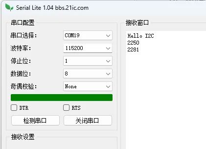
The values read are the same as those written.
Finally, here is the complete test code:
#define SCLK_PIN 8#define SDIO_PIN 9void I2C_Start(){ // Set the two pins used for I2C to output mode pinMode(SCLK_PIN, OUTPUT); pinMode(SDIO_PIN, OUTPUT); // When SCL is high, a falling edge on SDA represents the start signal digitalWrite(SDIO_PIN, 1); digitalWrite(SCLK_PIN, 1); digitalWrite(SDIO_PIN, 0);}void I2C_Stop(){ pinMode(SDIO_PIN, OUTPUT); // When SCL is high, a rising edge on SDA represents the stop signal digitalWrite(SDIO_PIN, 0); digitalWrite(SCLK_PIN, 1); digitalWrite(SDIO_PIN, 1);}void I2C_Write(uint8_t dat){ pinMode(SDIO_PIN, OUTPUT); // After pulling the clock line low, we can modify the data line's state digitalWrite(SCLK_PIN, 0); for(int i=0;i<8;i++) { digitalWrite(SDIO_PIN, (bool)(dat&0x80)); digitalWrite(SCLK_PIN, 1); // Send data when high dat=dat<<1; digitalWrite(SCLK_PIN, 0); // Pull low to prepare for the next bit's sending }}uint8_t I2C_Read(){ uint8_t dat=0; pinMode(SDIO_PIN, INPUT); for(int i=0;i<8;i++) { digitalWrite(SCLK_PIN, 1); // Read data while the clock is high dat=dat<<1; if(digitalRead(SDIO_PIN)) { dat=dat|1; } digitalWrite(SCLK_PIN, 0); // Pull low to prepare for the next bit's reading } return dat;}bool I2C_RACK(){ bool ack; pinMode(SDIO_PIN, INPUT); digitalWrite(SCLK_PIN, 1); // Receive acknowledgment signal; when the clock is high, the slave sends out the acknowledgment signal ack = digitalRead(SDIO_PIN); digitalWrite(SCLK_PIN, 0); // Pull low after reading the acknowledgment signal. return ack;}void I2C_ACK(){ pinMode(SDIO_PIN, OUTPUT); digitalWrite(SDIO_PIN, 0); // Send acknowledgment signal to the slave, pull the data line low, then pull the clock high to let the slave read this acknowledgment digitalWrite(SCLK_PIN, 1); digitalWrite(SCLK_PIN, 0); // After executing the acknowledgment, pull the clock line low to prepare for the next action.}void I2C_NACK(){ // Non-acknowledgment signal: the master no longer acknowledges the slave, releases the data line by pulling it high, then gives the clock a cycle signal (pull high then low) pinMode(SDIO_PIN, OUTPUT); digitalWrite(SDIO_PIN, 1); digitalWrite(SCLK_PIN, 1); digitalWrite(SCLK_PIN, 0);}uint16_t read_reg(uint8_t reg){ uint16_t dat=0; reg=(reg<<1)|1; I2C_Start(); I2C_Write(0x80); I2C_RACK(); I2C_Write(reg); I2C_RACK(); dat=I2C_Read(); dat=dat<<8; I2C_ACK(); dat=dat|I2C_Read(); I2C_NACK(); I2C_Stop(); return dat;}void write_reg(uint8_t reg, uint16_t dat){ reg=(reg<<1); I2C_Start(); I2C_Write(0x80); I2C_RACK(); I2C_Write(reg); I2C_RACK(); I2C_Write(dat>>8); I2C_RACK(); I2C_Write(dat&0xFF); I2C_NACK(); I2C_Stop();}void setup() { Serial.begin(115200); Serial.println("Hello I2C"); write_reg(0x02,0x2250); Serial.println(read_reg(0x02),HEX); write_reg(0x02,0x2281); Serial.println(read_reg(0x02),HEX);}void loop() {}Did you learn how to manually write the IO simulation I2C timing code after reading this article?