Click the card below to follow Arm Technology Academy
This article is selected from the Extreme Technology column “Arm Technology Blog” and will help you better learn about the evolution of the Arm Mali GPU architecture. At the beginning of the year, I had the opportunity to research the evolution of the ARM Mali GPU architecture, which has gone through four generations: Utgard, Midgard, Bifrost, and Valhall. I feel that its evolution is a microcosm of the development of large GPU architectures, so I wrote this article to record my insights. I do not intend to introduce the details of each generation’s architecture one by one, but rather to discuss the development of each generation of GPUs in relation to the Shader processors. Students interested in the details of each generation’s architecture or those who wish to understand the overall picture can refer to the sources【2】【3】【4】【5】.
I.Shader Processors
After the development of graphic APIs to OpenGL 2.0, the graphics processing pipeline broke free from the previous fixed model and achieved a high degree of customization. Shaders were introduced for various stages of the graphics pipeline, such as Vertex Shaders, Fragment Shaders, and later Geometry Shaders, Tessellation Shaders, and Compute Shaders. Each Shader is a small program written by the user, and executing these small programs is the job of the Shader processors in the GPU.
The Shader processor, as a core component, is crucial to the GPU’s performance and has undergone the most intense evolution. Each generation of Mali GPUs makes significant adjustments to the Shader processors to adapt to the development of graphic APIs and applications. Here, I will focus on two major changes: the unified processor architecture and TLP-driven architecture design.
II.From Independent to Unified
The first generation Utgard architecture had two types of Shader processors: GP – which executes Vertex Shaders, and PP – which executes Fragment Shaders. They used different hardware architectures and instruction sets, so the compiler would compile different Shaders into machine code for their respective Shader processors to execute.
Vertex Shaders are executed once for each vertex, while Fragment Shaders are executed once for each pixel. Generally, the execution count of Fragment Shaders is greater than that of Vertex Shaders; moreover, many graphical effects are more complex in Fragment Shaders than in Vertex Shaders. Thus, Utgard has one GP paired with multiple PPs, such as one GP with four PPs, which is MP4, and can go up to MP8. The hardware design of a single PP is also relatively more complex than that of a GP.
This independent Shader processor architecture means that the computing power between Shader processors cannot be shared. When the computational demand of one Shader far exceeds that of another, the other Shader processor can only wait idly, resulting in decreased utilization. Furthermore, as new types of Shaders are added to the graphic APIs, designing a processor for each type of Shader continuously increases software and hardware complexity. However, these Shaders are almost identical in terms of pure computation and can reuse most of the design, eliminating the need for a separate setup for each Shader.
Therefore, starting from the Midgard generation, a unified Shader processor architecture was adopted. Different types of Shaders share the computational parts as a unified Shader processor, while fixed-function operations such as vertex interpolation and rasterization are kept separate. This way, each type of Shader can fully utilize all processors, improving hardware utilization.
III.From ILP to TLP
ILP (Instruction Level Parallelism) and TLP (Thread Level Parallelism) have coexisted to some extent in each generation of Shader processor architectures, but the trend is that the weight of TLP has gradually increased.
In the Utgard and Midgard architectures, TLP was limited to the processor level. Shader processors operate like a core of a CPU, running one vertex or pixel Shader at a time. The number of processors equals the number of threads. For example, the Mali400MP4 has four PPs, which can process four pixels’ fragment shaders in parallel. Each processor entirely adopted ILP to focus on optimizing single-thread performance.
We can glimpse the design of ILP from the VLIW (Very Long Instruction Word) instructions used in both architectures【6】. The instruction encoding of Utgard PP can be referenced【7】, which includes two vector processing units, two scalar processing units, a function processing unit, and a unit responsible for various data loading and execution control. This type of VLIW instruction is different from ordinary CPU instructions; one instruction can perform multiple operations. It corresponds to the pipeline structure in hardware, as shown in Figure 1. The pipeline is a sequence of stages in which a processor executes instructions, which can be divided into multiple stages.
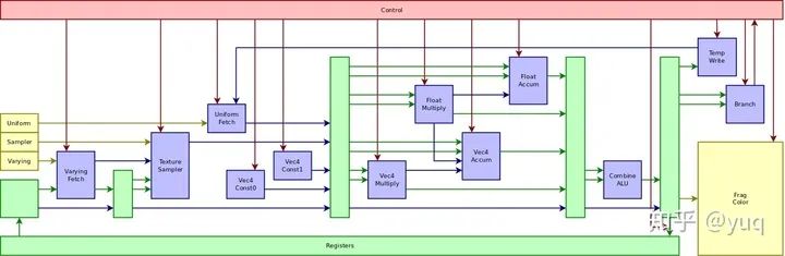
Figure 1: Utgard PP Processor Pipeline【7】
For instance, a series of operations: fetching texture data, then performing addition, followed by multiplication, and finally writing the result to memory. A RISC (Reduced Instruction Set Computing) generally requires four instructions, each with its own fetch, execute, and write-back steps; however, VLIW can string these operations together in one instruction. The fetched texture data does not need to be written into the register file but is directly passed to the addition unit, and the result of the addition unit is also directly passed to the multiplication unit, which then outputs to memory. Thus, the VLIW pipeline is longer, but by omitting intermediate steps, it becomes more efficient.
Ordinary CPUs improve single-thread performance through complex hardware designs that dynamically schedule the instructions to be executed, such as parallel execution and out-of-order execution. VLIW, on the other hand, relies on the compiler to statically schedule each operation during the compilation phase to fill the operations into the VLIW instruction units. Therefore, many early GPUs, including desktop and mobile versions, adopted VLIW to enhance ILP while simplifying hardware and reducing power consumption. However, this design places high demands on the compiler. How to schedule the operations in the Shader to fully utilize all operation units within a single instruction determines the execution efficiency of the hardware. Of course, the logic of the Shader itself also dictates whether there are enough operations that can be parallelized. These are limitations on the development direction of ILP.
Fortunately, graphical computation is a naturally data-parallel domain—there are a large number of primitives to compute, and the computation of each primitive can proceed independently, without relying on other primitives. Therefore, the computation of each primitive can be treated as a thread, and rendering a frame of graphics involves executing thousands of these threads. By utilizing a large number of threads, many operations can be executed in parallel without complex scheduling, achieving high hardware utilization. This is the starting point for TLP design in GPUs.
Starting from the Bifrost architecture, ARM also introduced TLP within a single processor. The method is to group a large number of threads into groups of four (later expanded to eight, then sixteen), and then run these groups within a single processor. Threads within the same group execute the same instructions, similar to SIMD (Single Instruction, Multiple Data). This way, there is no need to prepare a complete processor design for each thread; instead, multiple threads can share parts of the processor, except for the executors and registers. With more cores, the number of concurrently running threads significantly increases.
Moreover, to hide some operations, such as memory access delays, there is a pool of thread groups, which can prepare dozens of groups of threads ready to execute different instructions. When a group of threads cannot be executed immediately due to data access or other dependencies, the hardware scheduler can suspend that group and execute another group of threads. This is also an example of utilizing the number of threads.
However, the Bifrost architecture still incorporates many ILP designs, such as clause instructions (Figure 2): which group many serial instructions into a block—called a clause. A clause is the smallest unit scheduled by the hardware scheduler. Clauses can contain some accelerated operations, for example, when the output of an addition instruction is the input of a subtraction instruction, data can be transferred directly without going through the register file. Although the number of single instructions is reduced, there are still three computation units. Thus, the compiler still needs to consider the filling of single instruction units and the composition of multiple instructions into clauses.
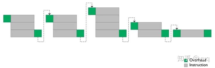
Figure 2: Bifrost Clause Instruction【4】
The Valhall architecture relies even more on TLP to enhance performance. To achieve this, it abandons clause instructions and multi-unit instructions that depend on software ILP characteristics, reducing scheduling granularity while also shortening the processor pipeline. As shown in Figure 3, Valhall’s processor has three computation units, including one FMA (Fused-Multiply-Add), one CVT (Convert), and one SFU (Special Function Unit). The thread group scheduler can find thread groups using different computation units for the current instructions from the thread group pool, allowing them to execute simultaneously across three computation units within four clock cycles. In contrast, Bifrost also has three computation units, but they belong to a long instruction, and ADD and Table are downstream of FMA, representing a serial structure, requiring eight clock cycles for this pipeline.
In comparison, Valhall further strengthens TLP, allowing a maximum of three thread groups to run simultaneously per processor, while Bifrost can only run one at most. Conversely, Valhall compresses three Bifrost processors into one, reducing control logic, which creates more space to increase the number of processors, thus also increasing TLP.
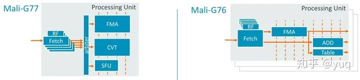
Figure 3: Comparison of Valhall and Bifrost Processors【5】
IV.Conclusion
In the history of GPU architecture, the unified Shader processor and TLP-driven architecture design are trends. GPUs from various manufacturers and generations have experienced this process to varying degrees. From an architectural standpoint, later GPUs are more advanced than earlier ones, but in the context of their time, early graphical applications had less complex Shader loads, and strict control over area and power consumption in mobile domain processors were the sources of their rationality.
V.References
1. Mali (GPU):https://zh.wikipedia.org/wiki/Mali_(GPU)2. Lima driver status update:https://xdc2019.x.org/event/5/contributions/328/attachments/420/670/lima.pdf3.ARM’s Mali Midgard Architecture Explored:https://www.anandtech.com/show/8234/arms-mali-midgard-architecture-explored4.ARM Unveils Next Generation Bifrost GPU Architecture & Mali-G71: The New High-End Mali:https://www.anandtech.com/show/10375/arm-unveils-bifrost-and-mali-g715.Arm’s New Mali-G77 & Valhall GPU Architecture: A Major Leap:https://www.anandtech.com/show/14385/arm-announces-malig77-gpu6.Very long instruction word:https://en.wikipedia.org/wiki/Very_long_instruction_wordA4%E5%AD%977.Mali ISA:https://gitlab.freedesktop.org/panfrost/mali-isa-docs/-/tree/master
Recommended Reading
-
Live | Designing a Music Player Based on Cortex-M0 on FPGA
-
How CPU Interacts with Memory
-
A Simple Interpretation of Cortex-M23/33 (Part 1)
Follow Arm Technology Academy