

1. Manual Routing Whenever Possible
Generally speaking, most PCB design software includes an auto-routing feature, but in reality, no auto-router can completely replace the skills, experience, and flexibility of a PCB Layout Engineer. (Kudos to manual PCB Layout Engineers)
In some cases, you can use auto-routing:
- After placing all components, you can use auto-routing to check your completion rate; if it is below 85%, you need to adjust your component placement.
- During routing, bottlenecks and other critical connection points may fall through the cracks, and you can use the auto-routing feature to identify them.
- When you are unsure how to start routing or encounter difficulties, you can use auto-routing as a source of inspiration.
In summary, routing is both a science and an art, and it is recommended to do manual routing as much as possible to ensure accuracy and reliability.
2. Understand Manufacturer Specifications
Before you start laying down copper traces, take the time to ask your manufacturer, if they have requirements for minimum trace width, trace spacing, and the number of PCB layers they can assemble.
By understanding this information in advance, you can set trace width and spacing values in your design rules, avoiding the need to re-route the entire PCB layout.
3. Choose Appropriate Trace Widths
The geometry of the traces (thickness and width) can ensure that the circuit operates normally under all environmental and load conditions.The traces on a PCB are used to transmit electrical signals, so they must have widths compatible with the currents passing through them.
The PCB Layout Engineer must determine the minimum width for each trace to avoid the risk of overheating the circuit board; this parameter directly affects the routing process as it reduces the available space on the PCB.
If available space is not an issue, it is recommended to use traces wider than the minimum to improve thermal management and reliability; traces on the outer layers can achieve better heat exchange and may therefore have smaller widths.
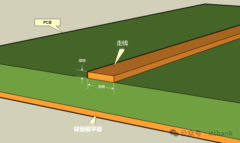
Trace Width
4. Leave Sufficient Space Between Traces and Pads
It is crucial to leave sufficient space between PCB traces and pads (as shown below) to avoid short circuits during PCB manufacturing or assembly.
Generally, it is recommended to leave appropriate gaps between each adjacent trace and pad, ensuring that there is always enough space around them without traces or pads to avoid the risk of electric shock.
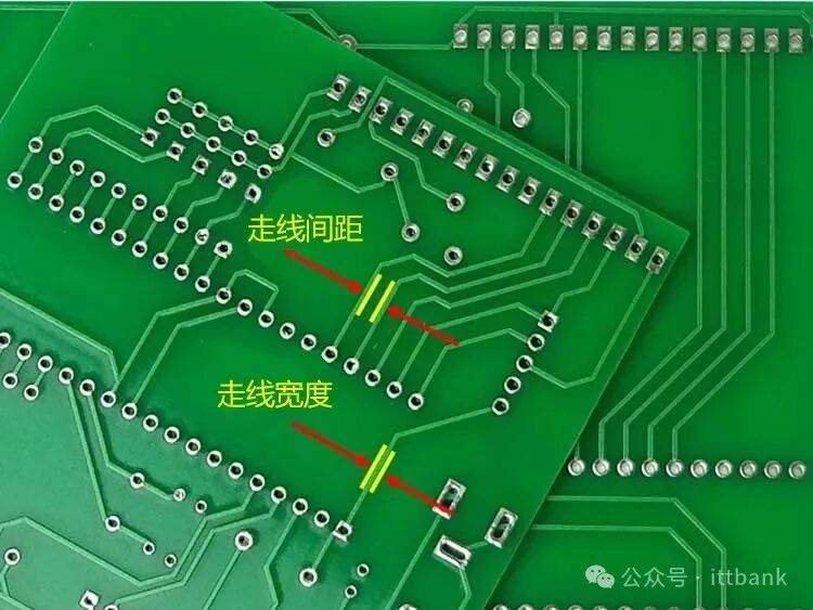
Trace Distance and Thickness
5. PCB Component Placement
The way components are placed determines the success of the PCB design.To place components correctly, you must fully understand their characteristics.
For example, thermosensitive electrolytic capacitors must be placed away from heat-generating diodes, resistors, and inductors.
Here are some simple rules of thumb:
- Pay attention to multi-pin components, as they occupy significant space.
- Keep components oriented in the same direction.
- Consider the function of each component and its relationship with other components before placement.
- If components have already been procured, it is advisable to print the layout on paper according to size and check if the components fit.
For more tips on PCB component placement, see the following:
How to Place PCB Components? 14 Tips for Component Placement Summarized, Illustrated and Easy to Understand
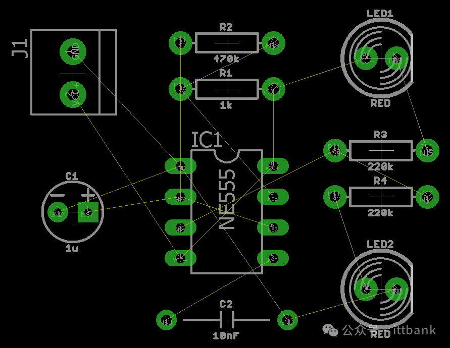
PCB Component Placement Diagram
6. Keep Analog and Digital Traces Separate
PCB traces carrying digital signals, especially high-frequency signals, must be kept separate from those carrying analog signals.Digital signals (such as address or data buses) are typically transmitted on parallel traces, which may introduce capacitive coupling and interference between signals.
This can lead to noise generation; generally, it is difficult to resolve this issue without altering the PCB, so it is recommended to keep high-frequency digital traces away from traces you do not want to be affected by noise.
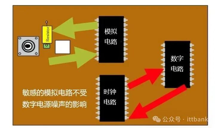
Keep Analog and Digital Traces Separate
7. Pay Attention to Ground Layers
Every PCB requires at least one ground layer, as it provides a common reference point for all traces to measure voltage.
Conversely, if you choose to route each individual trace to ground instead of using a ground plane, you will end up with numerous different ground connections, each with its own resistance and voltage drop.
The simplest and most linear solutionisto create a solid ground layer, which can be an entire copper area, and in the case of multilayer boards, it can even be an entire layer.
Placing a ground layer beneath signal-carrying traces helps reduce their impedance and improve noise immunity; it is recommended to place power and ground layers in the innermost layers of the circuit board to keep them symmetrical and centered, preventing PCB warping.
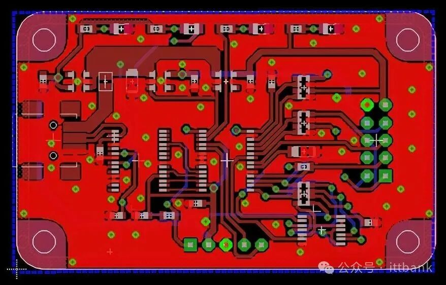
Solid Ground Plane, Shown in Pure Red, All Holes Can Be Easily Connected
8. Leave Sufficient Space for Traces and Mounting Holes
During the component placement process, you should first place all the through-hole components; have you left enough space between other components and all traces connecting them?
If you haven’t done this, there may be a risk of electric shock on the PCB, and relying on the solder mask as the only insulator does not guarantee safety.
When using through-hole components, remember to leave a margin of space beyond the physical size of the mounting holes to protect them from nearby components and traces.
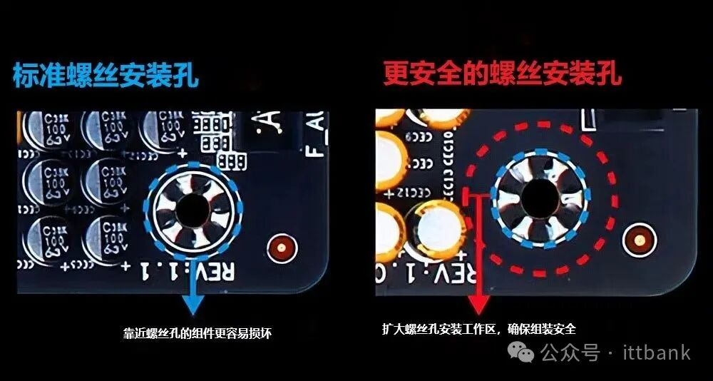
Keep Traces and Components Away from Mounting Holes to Avoid Electric Shock Risks
9. Alternate Trace Directions
Everyone should know that connections between components should be as short and straight as possible.If most traces on a layer follow one direction (e.g., horizontal), then prioritize traces in the perpendicular direction (e.g., vertical) for adjacent connections, as this can reduce crosstalk between tracks.
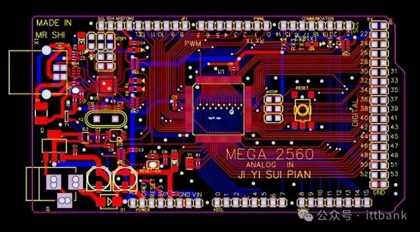
Compatible Arduino Mega 2560 Board
10. Avoid Capacitive Coupling
To reduce capacitive coupling caused by traces placed above and below large ground planes, ensure that traces allocated for power and analog signals are arranged on dedicated layers.
Decoupling capacitors are relatively robust yet inexpensive components that are typically present, and decoupling the power lines and compensating for component tolerances is essential. The traces for decoupling capacitors should be very short and as close as possible to the component’s power terminals.
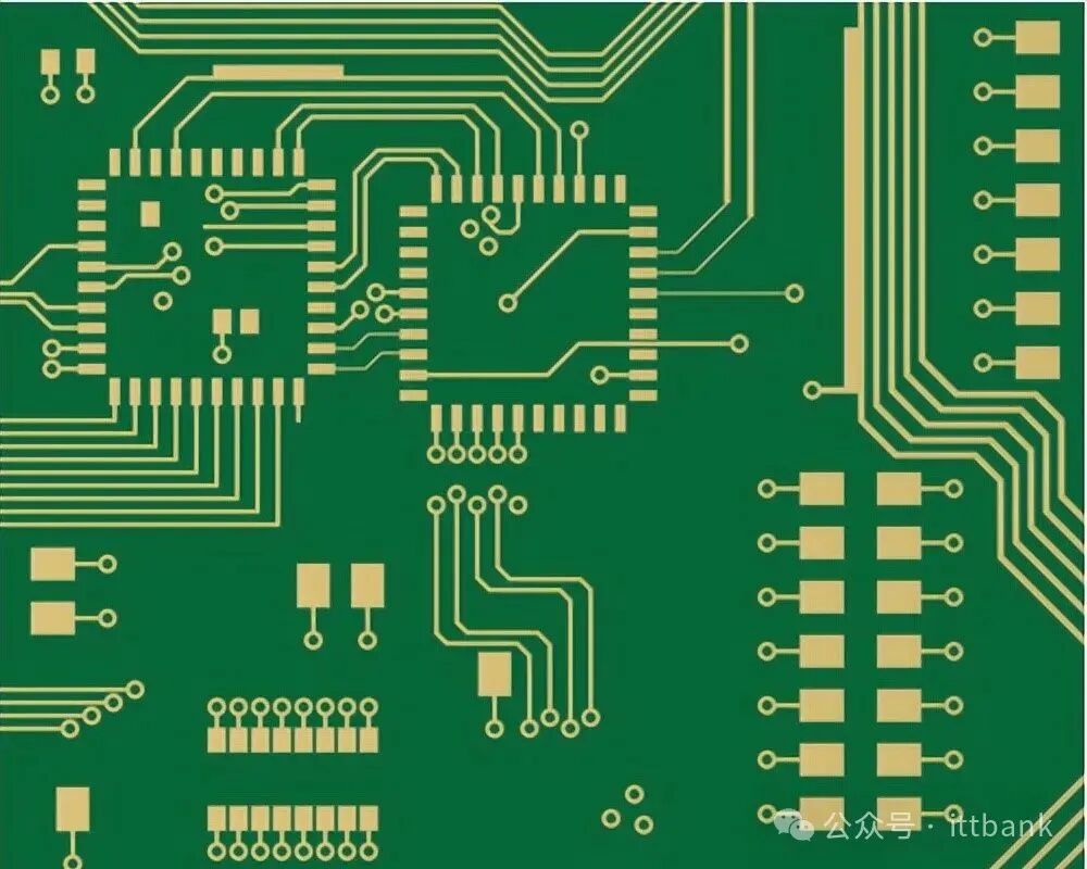
Shorten Traces to Reduce Capacitive Coupling
11. Place Thermal Vias and Pads
To improve thermal management, it is recommended to use thermal pads on through-hole components to simplify the soldering process and enhance heat dissipation.It is advisable to insert thermal pads when traces or holes connect to ground or power layers.
Thermal vias are also very important, as they not only provide electrical connections between layers but also transfer heat from the hottest components to the outside.By placing thermal vias under chip packages, you can lower the operating temperature of components, thereby improving circuit reliability and durability.
If it is necessary to dissipate heat from a high-power component (such as an integrated circuit (IC)), placing multiple vias beneath the IC chip can lower the component’s operating temperature, making the design appear more reliable.
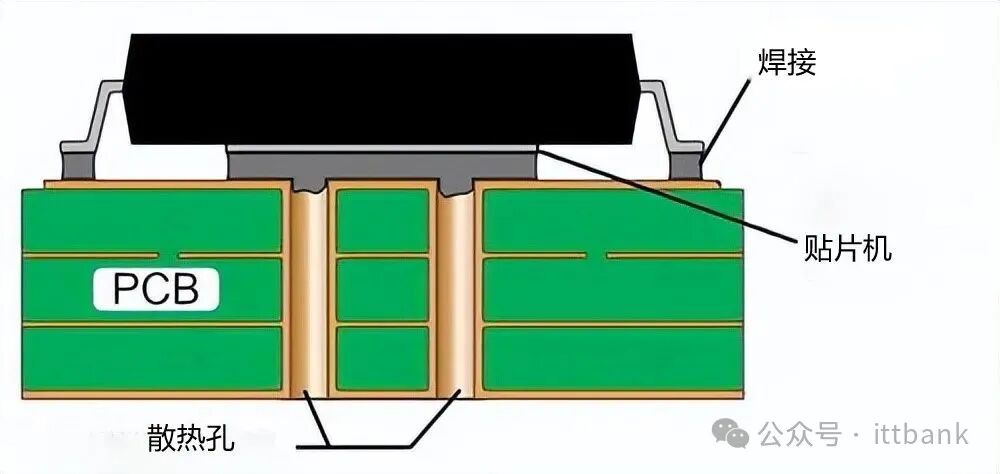
Using a Set of Vias Beneath the Integrated Circuit Chip to Transfer Heat from One Side of the Circuit Board to the Other
12. Ground and Power Traces
Traces related to power and ground signals should be thicker than those carrying digital or analog signals, allowing them to carry larger currents, which can be easily identified through simple visual inspection, thus reducing the likelihood of connection errors between signal and power lines.
A common rule is to use a width of 0.040 inches for ground and power traces and 0.025 inches for all other traces.
If you do not make the power and ground traces wider than the average width, a large amount of heat trying to flow through those narrow spaces may eventually burn the wires and damage the PCB.
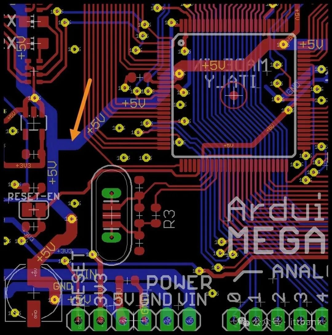
Compared to all signal traces connected to the integrated circuit, you can see that the +5V power trace is wider.
13. Utilize the Silkscreen Layer
The silkscreen layer that comes with the PCB can be used to mark the information you want to label..
- Do not use too much text, as it takes up space.
- There is no need to write down all available information; for example, it is absolutely unnecessary to label resistance values.
- If allowed, the text can be larger for clearer printing.
- Do not label bare copper pads that need to be soldered, as the ink may obstruct the flow of solder, leading to poor joints.
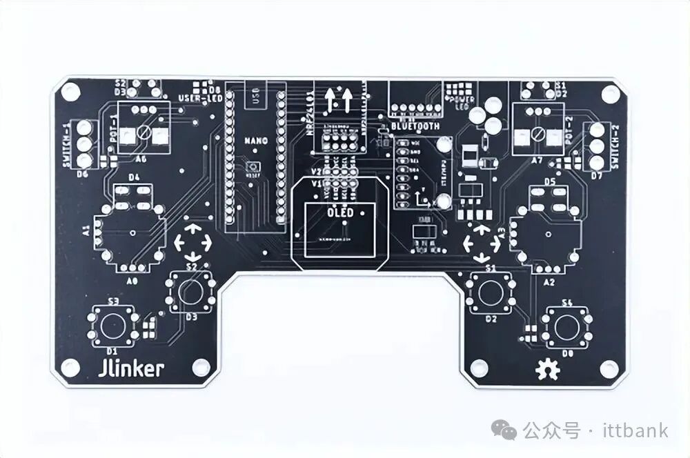
PCB Silkscreen
14. Avoid 90° Angles
Engineers should know that sharp angles and right-angle bends can cause problems at high frequencies, leading to discontinuities that can damage signal integrity through increased crosstalk, radiation, and reflection.
In the image below, several traces have replaced right angles with two 45° angles.
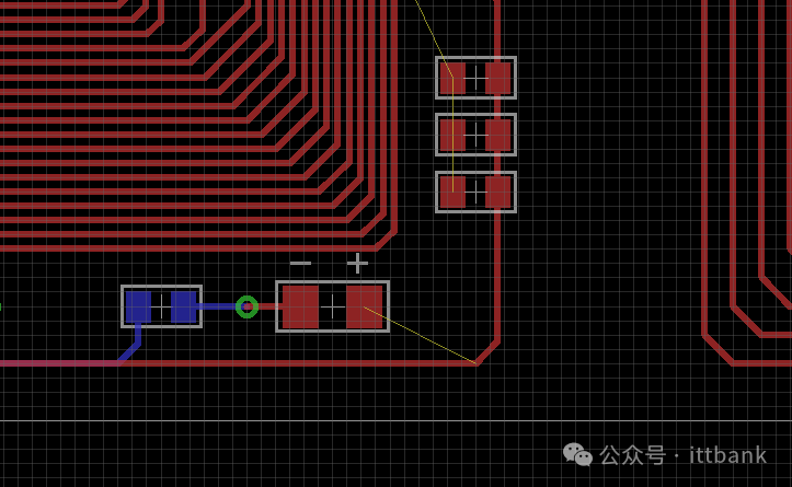
One Method to Avoid Right Angles
If you are an engineer, you may often hear not to use 90° angles; when your circuit board has a bunch of sharp right-angled traces, the outer corners of 90° may be etched narrower than your standard trace width, which can easily lead to PCB short circuits.
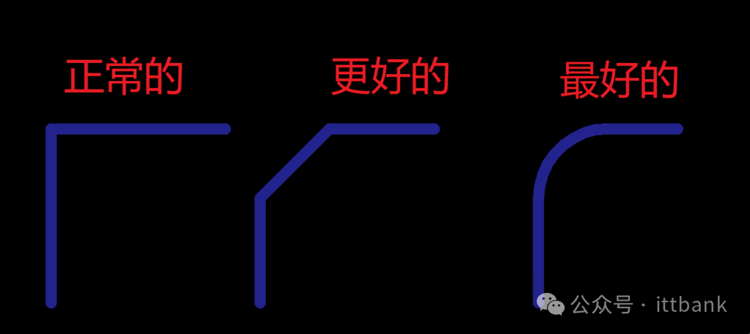
Trace Angles
Traces running through the entire PCB and around components should ideally be at a 45° angle.