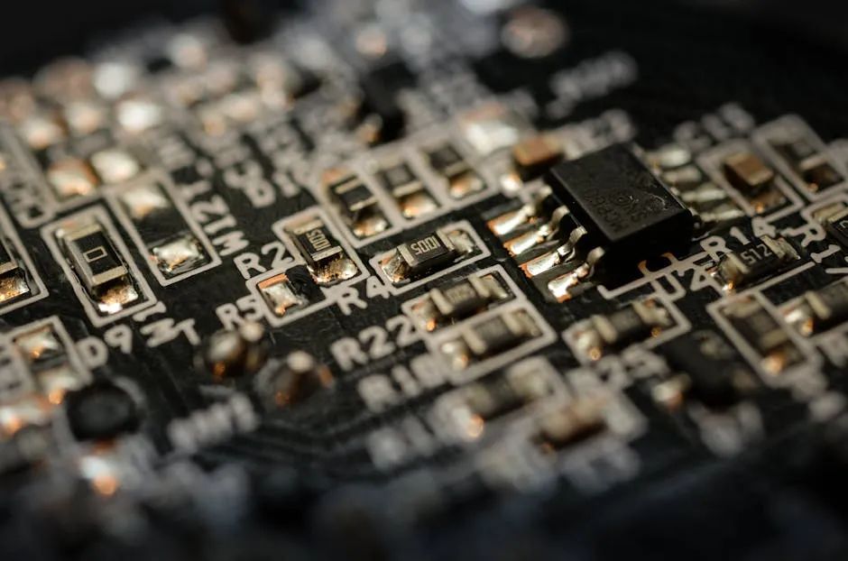
In the FPGA (Field Programmable Gate Array) design process, adjusting pins is a crucial task that directly relates to the stability and performance of the design. This article will discuss several aspects to pay attention to when adjusting FPGA pins!

1. Do Not Adjust VRN/VRP Pins Arbitrarily
When the VRN (Reference Negative Voltage) and VRP (Reference Positive Voltage) pins are connected to pull-up/pull-down resistors, these pins provide the reference voltage required by the DCI (Dynamic Current Adjustment) internal circuit. Adjusting these pins may cause the DCI internal circuit to fail to match the external reference resistance correctly, thereby affecting the I/O output impedance.
2. Pin Adjustments Between Banks of the Same Voltage Must Be Coordinated with Customers
Generally, pins between banks with the same voltage level can be interchanged. However, some customers may have specific adjustment requirements within certain banks. Therefore, it is essential to communicate and confirm with customers before making adjustments to avoid unnecessary rework.
3. Differential Pair Pins Must Not Be Interchanged
In differential signal transmission, the “P” (positive) and “N” (negative) pins correspond to the positive and negative ends of the differential pair, respectively. These two pins must not be interchanged; otherwise, the integrity of the differential signal will be compromised, leading to a decline in signal quality.
4. Global Clock Pins Fixed to P Ports
Global clock signals should be placed at the P ports of the FPGA’s global clock pins. These pins are specifically designed to ensure the stability and low latency of clock signals. Arbitrarily adjusting global clock pins may lead to a decline in clock signal quality, affecting system performance.
This article is an original piece by Wanyi Corporate Training; please indicate the source when reprinting!
Submissions/Recruitment/Advertising/Course Cooperation/Resource Exchange; please add WeChat: 13237418207