Researchers from Uppsala University and the University of Gothenburg have proposed a new type of anti-glare screen that can achieve extremely high pixel density. This technology is expected to overcome one of the main shortcomings of electronic ink technology, thereby promoting the widespread application of low-power, high-resolution displays.
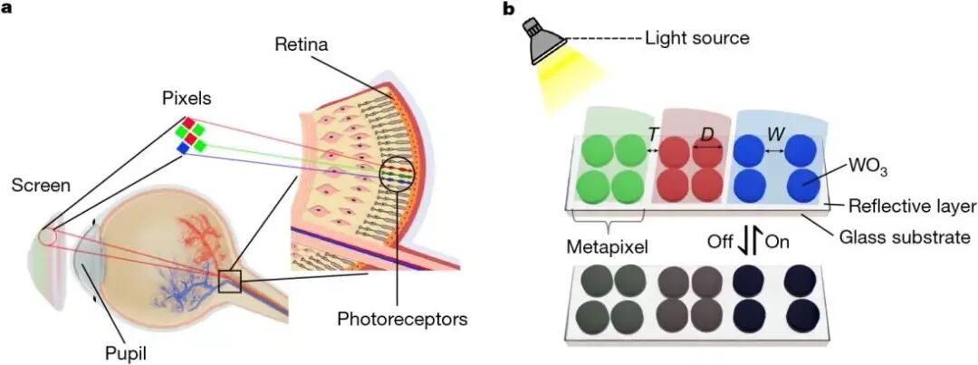
It is reported that this manufacturing process, named “retina E-paper,” utilizes electrochemical reduction to induce a reversible insulator-metal phase transition in tungsten trioxide nanodisks, allowing for precise control of the screen’s reflectivity and contrast at a very small scale. The resulting electronic paper can have pixel sizes as small as 560 nanometers, even smaller than some bacteria, with a pixel density exceeding 25,000 pixels per inch (PPI).
Theoretically, this technology could achieve a resolution far exceeding 4K on a screen the size of a contact lens.
In comparison, the pixel density of most iPhone models is about 460 PPI, while many high-resolution tablets or PC monitors have pixel densities slightly above 200 PPI. On the other hand, the latest electronic ink screens on the market can reach 300 PPI in black and white mode, but the resolution is typically halved in color mode.
Like other electronic ink screens, “retina E-paper” offers better contrast and visibility in direct sunlight compared to LCD or LED displays, while consuming less power. Researchers estimate that its power consumption when displaying static images is about 0.5 milliwatts per square centimeter, and about 1.7 milliwatts when playing videos, which is significantly lower than conventional electronic ink panels.
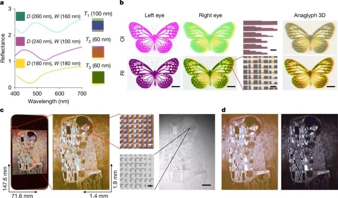
Although “retina E-paper” supports color display and anaglyph 3D effects, its refresh rate may not match that of traditional display technologies. Researchers state that its refresh rate can exceed 25Hz, but did not specify an upper limit. Currently, commercial electronic ink displays can reach up to 60Hz, while LED displays can show hundreds of frames per second.
Additionally, physicists from Julius-Maximilians-Universität Würzburg in Germany recently published another study proposing a method to reduce OLED pixels to just 300 square nanometers. If this technology is applied to wearable devices, it could theoretically integrate a 1080p resolution panel within a space of 1 square millimeter, with a pixel density potentially exceeding 55,000 PPI. However, this technology currently can only display orange, and its commercial prospects remain unclear.
Source: IT HomeHigh-performance barrier film projects,foldable screen OCA material projects, electronic paper module projects, chip testing projects, Mini/MicroLED device projects, semiconductor precision testing projects, etc. are open for investment and financing services. Please add WeChat for communication!