
After cloud computing, edge computing will become a new growth point in the IoT market over the next decade, which is an undeniable fact. According to market research firm Gartner, by 2025, 75% of data will be generated at the network edge, meaning that the distribution of computing resources in the entire smart world is shifting towards the “edge”.
Unlike traditional cloud computing architectures that centralize all computing resources in the cloud, edge computing places more computing tasks at the network edge. This computing architecture has unique advantages in reducing latency, avoiding bandwidth consumption from large data transfers, and protecting local sensitive data security.
Especially with the popularization of artificial intelligence (AI) applications, the model of “training in the cloud and inferring at the edge” has been widely recognized. By deploying trained machine learning models in edge devices, these devices can quickly and efficiently perform AI inference tasks, accelerating the deployment of more AI applications.
International telecom consulting firm STL Partners predicts that the potential market for edge computing will rapidly rise from $9 billion in 2020 to $445 billion by 2030, with a compound annual growth rate of up to 48%! Such a booming market also raises higher demands for players involved—if you want to keep up with the pace of market development, your edge AI development must also be able to accelerate.

Edge AI Drives Adaptive Computing
To accelerate application development, a prerequisite is to choose a fast and good “vehicle”—for edge AI development, this means selecting a development platform that can flexibly “accelerate”.
An AI inference application requires acceleration for the AI processing part, as well as meeting the functional requirements for non-AI preprocessing and postprocessing, meaning that the overall application process needs to be optimized.
For such development needs, using a general-purpose CPU with a single architecture, while flexible and scalable to support different application requirements, is clearly insufficient for accelerating the overall application process. On the other hand, developing dedicated ASICs or ASSPs for AI applications can provide highly optimized implementation solutions with high determinism and low latency, but it faces challenges such as long development cycles and high R&D costs. Meanwhile, using fixed dedicated chip architectures faces an even more severe challenge: the technological iteration speed of AI models far exceeds the chip development cycle, which can lead to chips becoming obsolete as soon as they are developed, resulting in irrecoverable sunk costs.
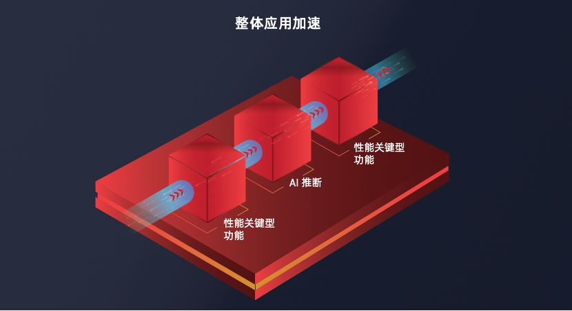
Figure 1: AI inference applications require overall application acceleration across the entire process
(Image source: AMD)
Faced with diverse edge applications and rapidly iterating AI technologies, since neither general-purpose CPUs nor dedicated chips can meet the requirements, a new development platform is needed to fill the gap—this is the adaptive computing platform based on programmable logic.
The so-called adaptive computing platform is a heterogeneous computing platform that integrates one or more embedded CPU subsystems, I/O, and other peripheral modules on FPGAs of different scales. This platform is also known as adaptive SoC or FPGA SoC, which combines the flexibility of embedded CPU subsystems with the required data processing acceleration performance provided through hardware programming. Therefore, developers can assign the right tasks to the right computing engines, ultimately accelerating AI inference while meeting the computational requirements of non-AI parts, thus providing ideal solutions for various specific applications. Moreover, even if workloads or standards evolve and change, adaptive SoCs can still be quickly configured and flexibly adapted as needed.
Because adaptive SoCs combine the advantages of performance and flexibility, they have developed into an important computing architecture in edge computing in recent years, and are a product line that FPGA manufacturers are focusing on. For example, AMD’s Zynq®UltraScale+TM MPSoC devices are representative of this.
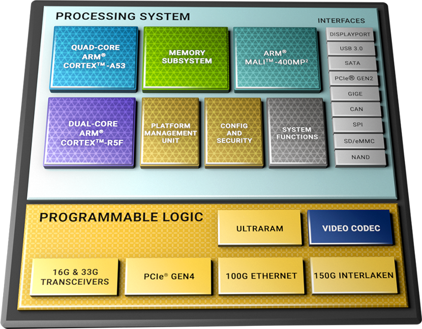
Figure 2: Zynq®UltraScale+TM MPSoC platform block diagram
(Image source: AMD)

Accelerating Adaptive Computing Application Development
It is evident that adaptive computing SoCs can provide users with three degrees of freedom: software programmability, hardware programmability, and the scalability of embedded platforms.
However, this “freedom” is also a double-edged sword for developers—it makes development more complex. This complexity arises from two aspects: first, the design and development process of FPGAs has a high threshold, and there are not many developers who can master it; second, overall optimization based on heterogeneous platforms often requires collaboration between multiple teams, making development time and costs difficult to control.
Therefore, although the “acceleration” capability of adaptive computing SoCs is evident, accelerating the application development process is not a simple task.
However, clever engineers always find ways to simplify the “not simple” tasks. In the matter of “accelerating adaptive computing application development,” AMD engineers have provided developers with a feasible and efficient method—solutions based on adaptive system modules (SOM).
The so-called SOM is a complete computing system that integrates a core chip along with peripheral memory, I/O interfaces, and other functional circuits. It is usually not used independently but is inserted into a motherboard (i.e., a larger edge application system) through connectors to realize a specific complete application.
The benefits that SOM brings to developers can be summarized in three points:
#1
First, SOMs are products that have undergone rigorous debugging, testing, and validation, so the development process does not need to start from lower-level chips, saving a lot of time and costs.
Second, SOMs have strong scalability; by inserting different system boards, customized solutions can be achieved, providing greater flexibility and usability in system design.
#2
#3
Additionally, SOMs are mass-producible and have been comprehensively optimized in terms of cost-effectiveness and reliability, making them suitable for use in mass commercial products.
These advantages address the “pain points” faced in adaptive computing application development, so designing an adaptive SOM and utilizing it to accelerate adaptive computing, empowering edge AI solutions, becomes the key “entry point” to the edge AI “highway”.

AMD’s Adaptive SOM
AMD’s Kria K26 SOM is the key “entry point” that everyone is looking for when entering the fast lane of edge AI.
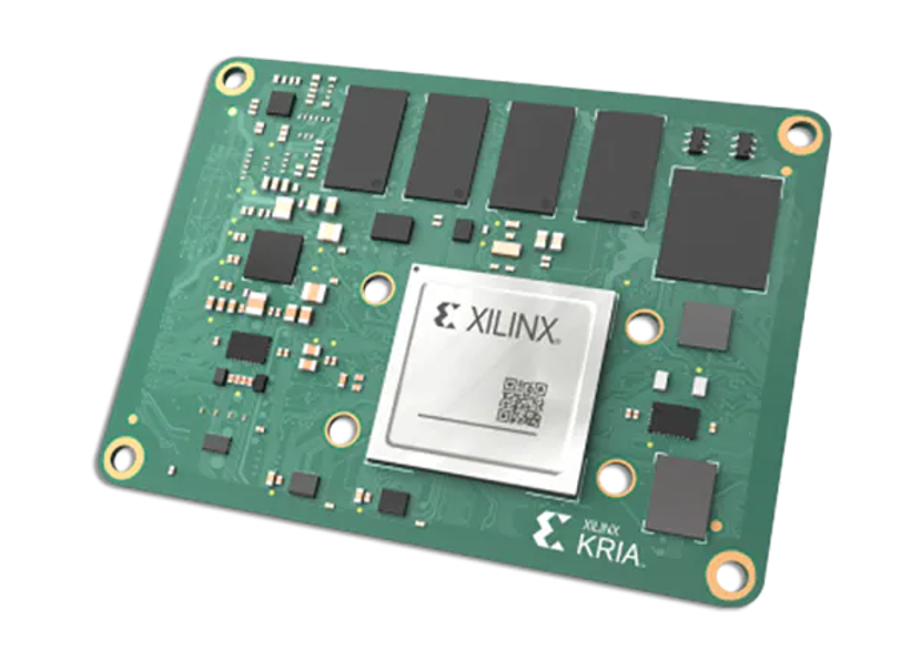
Figure 3: Kria K26 SOM
(Image source: AMD)
This SOM is based on the Zynq UltraScale+ MPSoC architecture, featuring a 64-bit quad-core Arm Cortex-A53 application processor group, along with a 32-bit dual-core Arm Cortex-R5F real-time processor and an Arm Mali-400MP2 3D graphics processor. The SOM also includes 4GB of 64-bit DDR4 memory and QSPI and eMMC storage.
Kria K26 SOM can provide 256,000 system logic units, 1,248 DSPs, and 26.6Mb of on-chip memory. This allows users to obtain rich resources and design freedom to implement visual functions in different applications, as well as additional hardware acceleration functions for machine learning preprocessing and postprocessing in programmable logic.
Moreover, this SOM also features a built-in video codec for H.264/H.265, supporting up to 32 concurrent encoding and decoding streams, as long as the total video pixels do not exceed 3840 x 2160P at 60FPS.
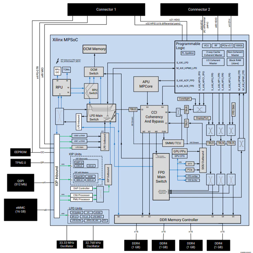
Figure 4: Kria K26 SOM block diagram
(Image source: AMD)
In terms of security, the Kria K26 SOM implements inherent secure boot functionality through the hardware root of trust built into the Zynq UltraScale+ architecture, with external TPM 2.0 extensions for measuring boot and compliance with IEC 62443 standards.
Additionally, the excellent I/O flexibility is another highlight of the Kria K26 SOM—it has a large number of 1.8V and 3.3V single-ended and differential I/Os, four 6Gb/s transceivers, and four 12.5Gb/s transceivers, facilitating the SOM’s support for more image sensors and various sensor interface types, including MIPI, LVDS, SLVS, and SLVS-EC, which are typically unsupported by ASSPs and GPUs.
Furthermore, users can implement standards such as DisplayPort, HDMI, PCIe, USB 2.0/3.0, and other user-defined standards through programmable logic.
In terms of form factor, the Kria K26 SOM measures 77mm x 60mm x 11mm, making it compact and easy to integrate into systems. AMD also plans to release smaller-sized SOMs in the future. Currently, the Kria K26 SOM is available in commercial and industrial versions, allowing users to choose based on the needs of their end applications.
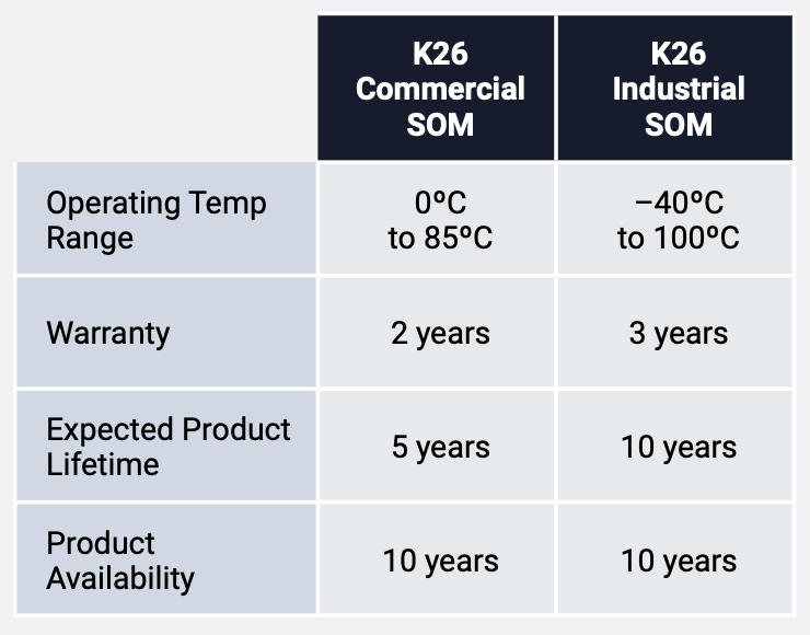
Figure 5: Comparison of commercial and industrial K26 SOM features
(Image source: AMD)
The Value of Kria K26 SOM
What kind of experience will using the Kria K26 SOM bring? How does it perform in practical design? This is certainly a concern for everyone.
First, from the perspective of simplifying the hardware design process, compared to traditional device-based designs, SOM-based designs eliminate the need for RTL/hardware design, device debugging, and circuit board design, starting directly from system-level design, thus greatly simplifying the development process—according to AMD’s analysis, SOM-based designs can shorten the time to market for new products by up to 9 months!
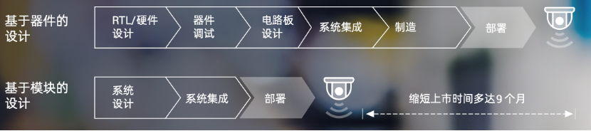
Figure 6: SOM-based design can shorten the time to market for new products by up to 9 months compared to chip-based design processes(Image source: AMD)
In terms of hardware performance, in an automotive license plate recognition (ANPR) application case provided by AMD, the solution based on the Kria K26 SOM excellently completed the acceleration and optimization of the entire process, including video decoding, image preprocessing, machine learning (detection), and OCR character recognition, showing significant advantages in computational performance, energy efficiency, and cost per video stream compared to SOM solutions based on GPU architecture (as shown in Figure 7). As the application of the K26 SOM expands, its performance potential will be increasingly realized.
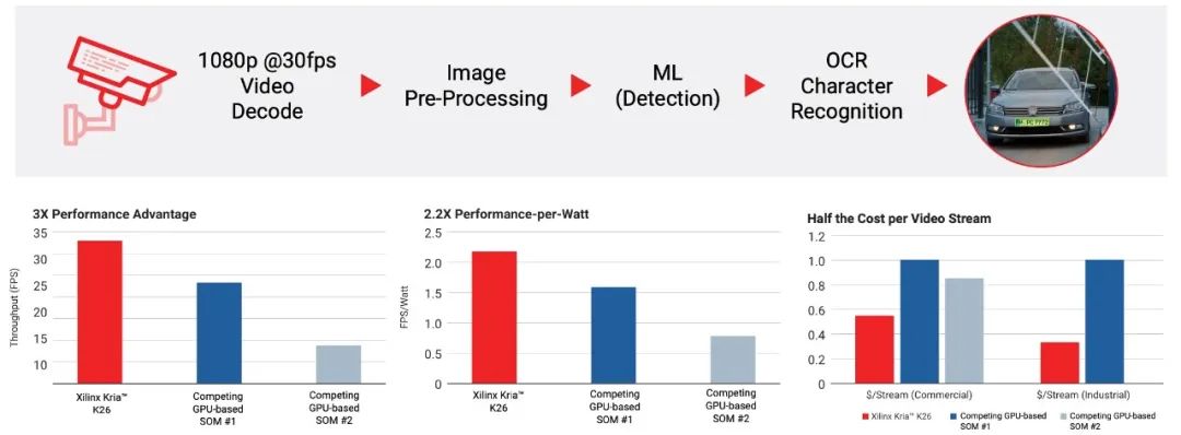
Figure 7: The K26 SOM shows significant performance advantages in the ANPR case (Image source: AMD)
It is particularly worth mentioning that the Kria K26 SOM not only brings numerous benefits to hardware developers but is also a boon for software developers. With the development of edge AI software tools, libraries, and frameworks that accompany the Kria K26 SOM, some design teams can utilize adaptive computing without the involvement of hardware engineers.
For software developers, the Kria K26 SOM and the comprehensive software platform provided by AMD allow them to develop in familiar environments such as Python, C++, TensorFlow, and PyTorch, providing an easy-to-use, out-of-the-box experience. Coupled with support from third-party software vendors in the AMD ecosystem, the performance and flexibility of edge AI development can be elevated to a higher level.

Quickly Experience Kria K26 SOM
To facilitate developers in quickly experiencing the powerful capabilities of the Kria K26 SOM and exploring its value, AMD has provided ready-to-use entry-level development kits for some typical edge AI applications.
The Kria KV260 is a vision AI entry kit developed specifically for visual applications, equipped with a non-production version of the Kria K26 SOM and an evaluation carrier board with a fan heat sink, providing multi-camera support through onsemi imaging system (IAS) and Raspberry Pi connectors. This development kit can also be expanded with rich sensor modules via PMOD.
Based on the KV260 vision AI entry kit, software and hardware developers can start and run applications within an hour without FPGA experience, quickly achieving mass deployment of visual AI applications on the Kria K26 SOM.
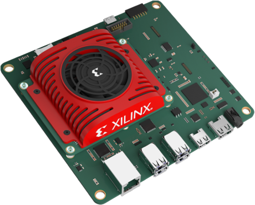
Figure 8: Kria KV260 Vision AI Entry Kit
(Image source: AMD)
The Kria KR260 Robot Entry Kit is a new development platform based on the Kria K26 SOM, featuring high-performance interfaces and native ROS 2 support, designed to provide a fast and easy development experience for robotics and embedded developers.
This development kit includes the Kria K26 SOM, a carrier board and cooling system, as well as power solutions, multiple Ethernet interfaces, SFP+ connections, SLVS-EC sensor interfaces, and a microSD card, targeting applications in factory automation, communication, control, and vision, especially in robotics and machine vision applications.
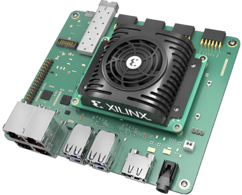
Figure 9: Kria KR260 Robot Entry Kit
(Image source: AMD)

Conclusion
Cloud computing has profoundly changed the landscape of the IT and IoT world, while the rise of edge computing is reshaping the rules of the game. In this trend, how to enable more and more edge AI applications to be deployed quickly requires a different kind of computing platform and corresponding development methods. Adaptive SOMs have thus emerged.
AMD’s Kria K26 SOM can put your edge AI development on the fast track, extending the scope of edge AI applications into broader fields.