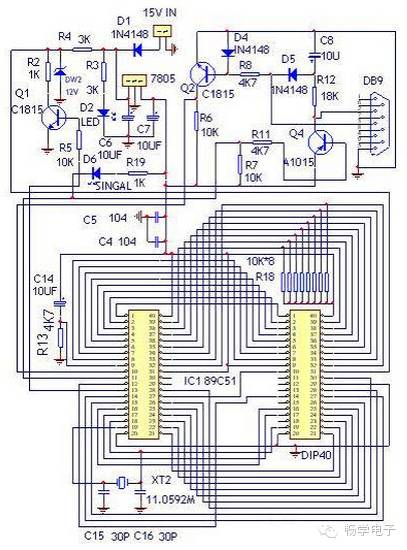
The AT89C51 is one of the most widely used 8051 microcontrollers, and importantly, it has the feature of being reprogrammable (FLASH). Generally, it can be rewritten 1000 times, providing a low-cost platform for beginners to experiment. To meet the hands-on needs of microcontroller enthusiasts, I spent half a month designing and successfully creating a simple programmer for the AT89C51/52/55 microcontrollers, referencing foreign materials. Due to the different programming timing of microcontrollers, this programmer only supports ATMEL’s AT89C51, AT89C52, and AT89C55 chips, and does not support Winbond or Philips compatible chips. Below is the circuit diagram of the microcontroller programmer.
Note: The component list can be found in the appendix.
Brief description of the working principle:
Q2, Q4, and several surrounding components form a level conversion circuit, saving one MAX 232 chip. In less demanding situations, this circuit can replace the MAX232 in microcontroller communications. Q1, R2, R4, and DW2 provide the programmer with a 12V programming voltage. Among them, R4 and R2 form a voltage divider; normally, the 13th pin (P3.3) of the AT89C51 chip outputs a high level, Q1 conducts, R2 (1K) pulls DW2 (12V) low, and at this time, the voltage of DW2 is divided by R4 and R2, approximately between 3-5V; when writing the program, the 13th pin (P3.3) of the chip outputs a low level, Q1 turns off, and DW2 (12V) is directly sent to pin 31 of the chip being programmed, thus providing the programming voltage. The programming voltage provided by the programmer on ATMEL’s official website is adjusted using an LM317 and requires two high-precision resistors, making the circuit complex and costly. This circuit has been proven to be very stable and reliable through hundreds of experiments conducted by myself.
The power transformer should be a 15V power supply, such as a common 3-12V adjustable DC power supply. Note that its no-load voltage should not be lower than 13V, and the filtering should be good; otherwise, programming may be unreliable.
*The chip should be installed in an IC socket, and another programmer should be used to burn the program EZ51.HEX before inserting it for debugging. If purchasing a burning socket is difficult, you can directly use an IC socket. The connection cable should be a 9-pin serial cable with one male and one female end. Note that some serial cables on the market have pins 2 and 3 crossed; it’s best to check with a multimeter to ensure they correspond one-to-one. If you don’t have a serial cable, you can dismantle an old serial mouse to make one, just ensure that pins 2, 3, and 5 are properly connected at both ends. This circuit does not have special requirements for components; resistors can be ordinary 1/8W carbon film, and I used 2SA1015 and 2SC1815 transistors; in fact, many low-power transistors can be used, such as 9014 and 9015. Just be careful of their pin arrangement differences. The diode 1N4148 can be replaced with 1N4004. Additionally, it’s best to select a 12V voltage regulator with an accuracy requirement of within 5%. The 11.0592M crystal should be tested if possible, as some crystals sold in the market do not oscillate.
The burning software for this programmer, EZ31.EXE, has a very simple interface; it is fully compatible with WINDOWS 9X-2000. It only has a few buttons: Open File (SEND), Read Chip (READ), Exit (EXIT), COM Selection, Lock Code (LOCK CODE), and Fast Verify (FAST VERILY). You’ll understand once you use it. Note that the version currently available for download is its upgraded version ez4.0, which automatically detects the port number and chip. It’s much easier to use! DIY installation steps:
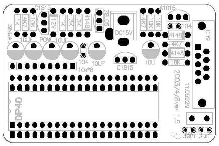
1: Install the resistors, a total of 11; after inserting the components, solder and trim the leads:
2: Install the diodes, three 1N4148 and one 12V voltage regulator DW2. Please carefully check the surface of the components for markings: the voltage regulator is marked with 12V, and be careful not to confuse them. Diodes are polarized; insert the black end of the diode towards the white side printed on the PCB: after inserting the components, solder and trim the leads:
3: Install 2 104 capacitors and 2 30p capacitors; 11.0592 crystal, these have no polarity and can be inserted arbitrarily:
4: Insert the transistors. Electrolytic capacitors and LEDs: note that these components are polarized; if reversed, it won’t work. The negative side of electrolytic capacitors and LEDs should face down. The transistors (2 2SC1815, one 2SA1015) and one 78L05 voltage regulator IC: their orientation can be seen on the PCB, with the flat side facing the half-circle direction.
5: Insert the resistor array (the end with a white dot is the common end, located near the edge of the PCB); the power socket and 232 socket do not need further explanation.
6: Insert the socket for the *chip.
7: Insert the burning socket. Since it and the *chip are facing each other, the *chip socket must be soldered first, followed by the burning socket. Otherwise, it will be difficult to solder later.
8: If you really can’t figure out the orientation of the components, please take a closer look at the photos above.
9: Finally, check if there are any incorrect inserts or shorts on the circuit board. Then debug according to the methods above. If there are no mistakes, it can usually be adjusted correctly on the first try.
Debugging:
After assembly, power on and check with a multimeter:
1. The output of the 7805 is 5V, and the power indicator D2 lights up. (In the figure, I used 78L05)
2. The voltage at DW2 is 3-5V.
4. Short the base of Q1 to ground, and the voltage at DW2 is 12V.
5. The voltages at pins 18 and 19 of U1 (89C51) are 2.2V and 2.1V, respectively; this voltage can be used as a basis for whether the circuit is oscillating.
Connect the programmer’s power supply and serial cable, and insert the chip to be programmed, then click COM1 or COM2 (depending on the actual connection; in this case, I connected COM2), and the window should display “89C51 Found” at the bottom right. At this point, the signal indicator D6 should light up every 2 seconds, indicating that it is working online.
Select a hex file to be programmed and start programming; if everything is normal, the displayed interface will be as shown in the above figure.
This is a super compact double-sided PCB; note that the *chip is installed on the reverse side. Therefore, the entire circuit board is only slightly larger than a matchbox, possibly the smallest programmer you can see. Isn’t it very beautiful?
Look at this picture: You must be able to handle it! There are less than 30 components in total, and it’s really easy; assembling one and testing it only takes half an hour.
Appendix: Component List
Part Type Designator Footprint
1K R19 axial0.3
1K R2 axial0.3
1N4148 D5 diode0.4
1N4148 D1 diode0.4
3K R3 axial0.3
3K R4 axial0.3
4K7 R13 axial0.3
4K7 R11 axial0.3
4K7 R8 axial0.3
10K*8 R18 (resistor array)
10K R7 axial0.3
10K R6 axial0.3
10K R5 axial0.3
10UF C8 RB.2/.4
10UF C14 RB.2/.4
10UF C7 RB.2/.4
10UF C6 RB.2/.4
11.0592M XT2 rad0.2 (crystal)
12V DW2 (voltage regulator)
15V IN 7257 (power input socket)
18K R12 axial0.3
30P C15 RAD0.1
30P C16 RAD0.1
104 C4 RAD0.1
104 C5 RAD0.1
A1015 Q4 to-126
C1815 Q1 to-126
C1815 Q2 to-126
IN4148 D4 diode0.4
LED D2 rb.2/.4 (LED)
SIGNAL D6 rb.2/.4 (LED)
DB9 232 socket
40PIN burning socket
40PIN IC socket (for *chip)
232 serial cable
PCB
89C51* chip
15V power supply