 This article is approximately 10,678 words long.
Author | Rick
1. Overview
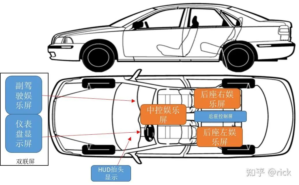
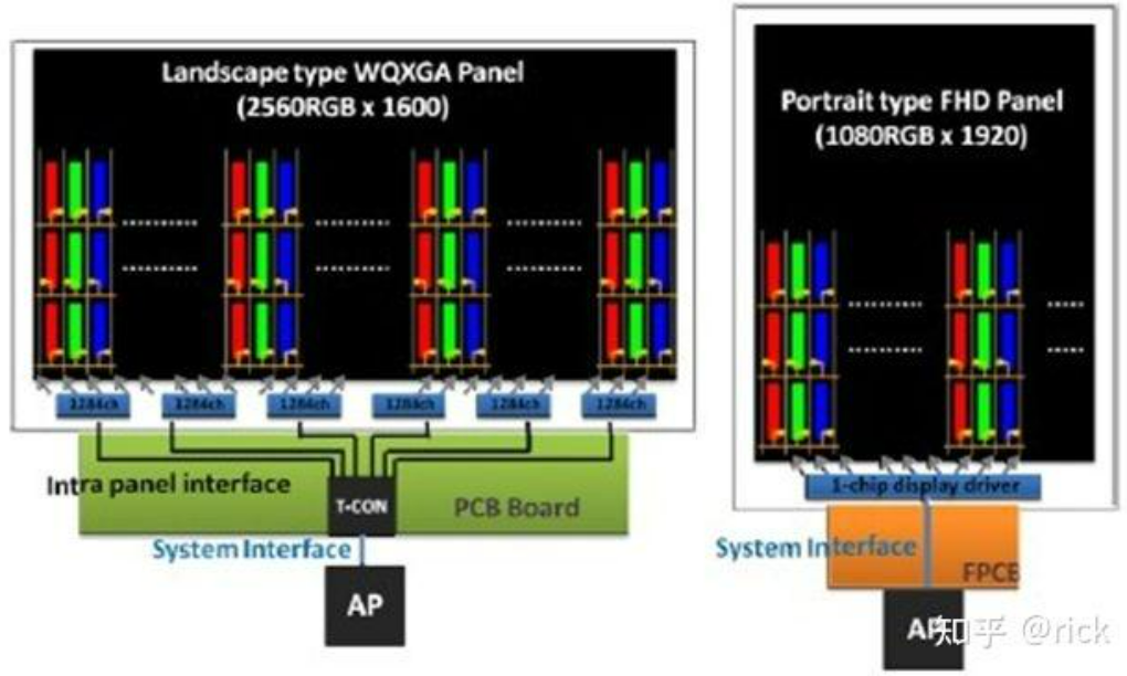
In the development of smart cockpits, the number of displays has increased, and the resolution and size of the displays have also grown larger. This is an irreversible trend. Traditional cockpit displays require a main chip to support each screen, which is not optimal in terms of functionality and cost. In the latest smart cockpit solutions, supporting multiple screens with a single chip is a necessary feature, with the distinction lying in the technology used. This section will mainly discuss the hardware-related technologies of the display subsystem in smart cockpits. As shown in the figure below, the displays that need to be supported within the smart cockpit include:
· Instrument Cluster Display IC· Passenger Infotainment Screen· Instrument Central Screen· Head Up Display (HUD)· Rear Control Panel (RCP)· Rear Infotainment Screen
-
· Instrument Display and Passenger Display
-
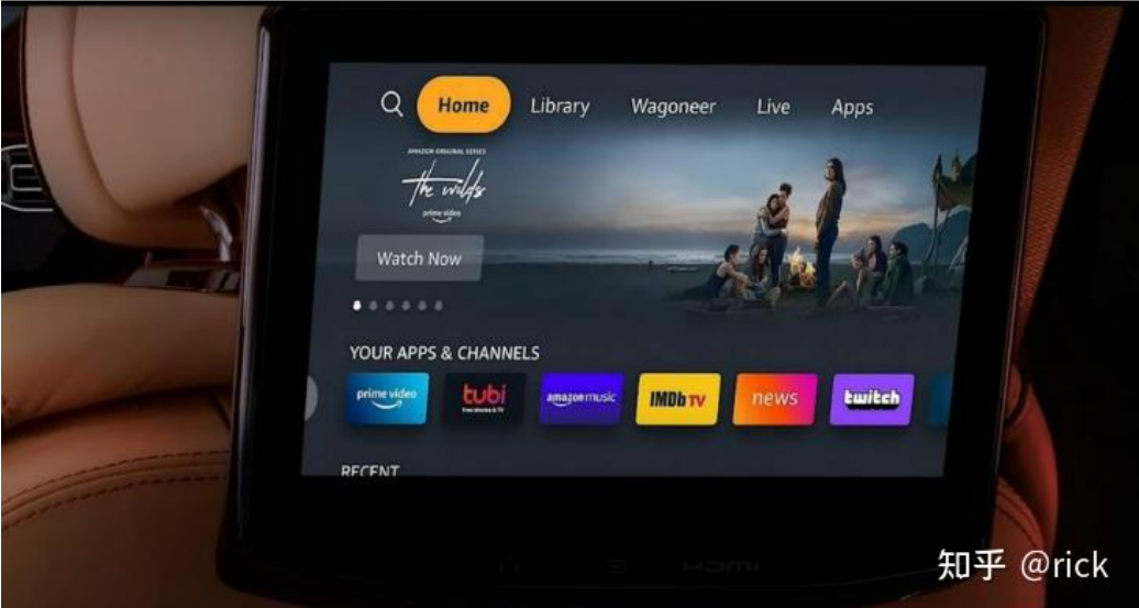
· Central Entertainment Screen
-
· HUD
-
· Rear Entertainment Screen
-
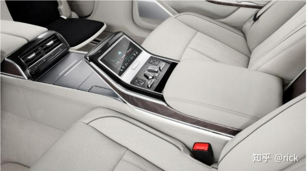
· Rear Control Screen
2. Cockpit Display Architecture
According to the latest trends in smart cockpit development, the vehicle display hardware technology needs to support multiple screens with a single chip. Using a CDC cockpit chip, it is necessary to meet the display requirements of multiple screens as described above as much as possible. This way, costs and power consumption can be minimized. The functionality that originally required multiple chips to support screens should be integrated into a single high-performance SOC chip, which is an objective requirement for the current development of smart cockpits.
A basic architecture of a vehicle display that meets the smart cockpit CDC multi-screen requirement is shown in the figure below:
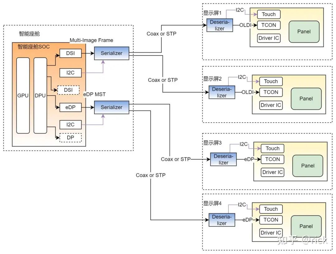
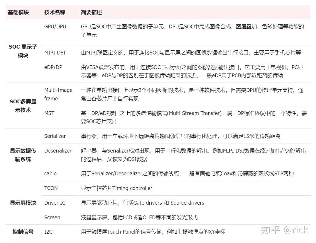
As shown in the figure above, the display subsystem of the smart cockpit CDC includes the following technologies:
3. Display Principles
This section will briefly introduce the basic principles of displays.
The display control system mainly consists of two types of chips: one is the driver chip responsible for driving the display and achieving row and column display, known as Driver IC. The other is the control chip responsible for task distribution and control of the Driver IC, known as TCON (Timing Controller).
The display driver chip, Driver IC, is an important component of the display imaging system, whose main function is to drive the pixels of the display to turn them on or off, and control light intensity and color.
The display driver chip is divided into source drivers (Source Driver) and gate drivers (Gate Driver). Gate Driver: connected to the gate terminal of the transistor, responsible for switching each row of transistors, opening an entire row of transistors at once during scanning; hence it is also called Row drivers. Source Driver: connected to the source terminal of the transistor. When a row of transistors is opened (ON) by the Gate driver, the Source Driver IC can load the control voltage for brightness, grayscale, and color onto each pixel in that row. Therefore, the Source Driver is also called Column Driver.
The structure of the Driver IC in the display can be referenced in the figure below:
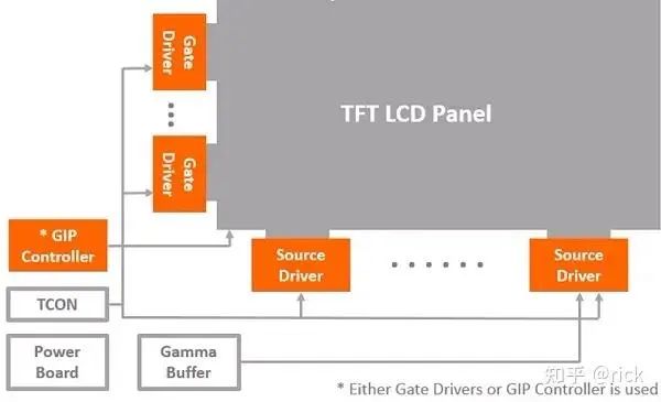
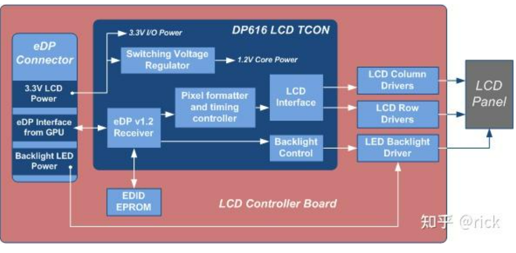
The timing control chip, TCON (Timing Controller), is the main control chip of the display module. It is mainly responsible for analyzing the signals from the CDC SOC, decomposing and converting them into signals that the Driver IC can understand, and then distributing them to the Source/Gate drivers for execution.
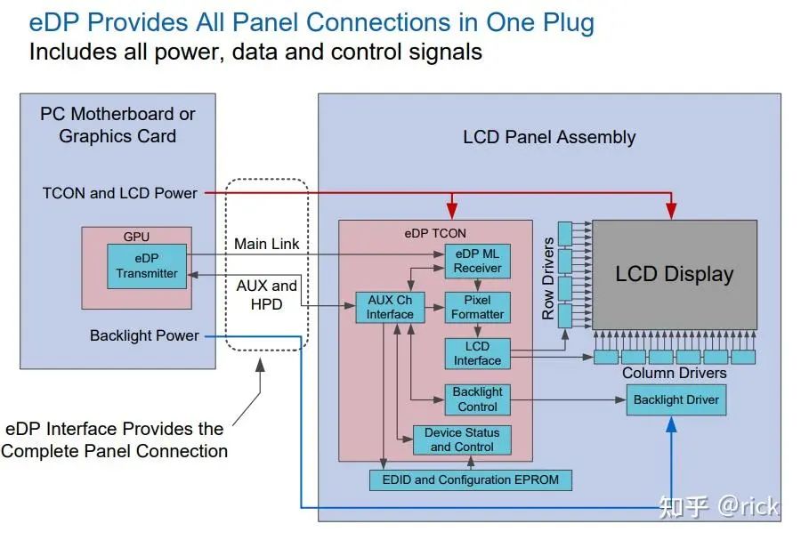
The figure below shows a typical eDP TCON interface system. The SOC transmits display data to the eDP TCON chip through the eDP channel.
TCON has two main functions:
-
1. Receive eDP signals from the SOC;
-
2. Generate row (sent to row drivers) and column (sent to column drivers) display signals, and send them to Row/Column Driver ICs according to the specified timing;
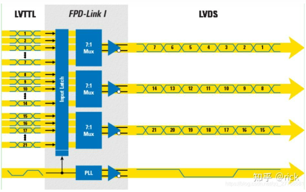
In the past, the signal transmission between T-CON and Gate/Source was mainly based on LVDS, but now the more popular versions are mini-LVDS (by Texas Instruments) and RSDS (Reduced Swing Differential Signaling by National Semiconductor). These two specifications are gradually becoming outdated, replaced by Advanced PPmL (Point to Point mini LVDS) and V-by-One HS with the accompanying standard CalDriCon. Therefore, at the T-CON, a transmitter that outputs mini-LVDS/RSDS/CalDriCon/Advanced PPmL signals is required, and at the Source/Gate IC, a corresponding receiver is needed.
When the signal is received, Row Drivers open the transistors row by row; while Column Drivers apply different levels of voltage to each column pixel in that row, thus achieving color and brightness differentiation of the pixels.
The difficulty in implementing the TCON chip lies in the need to generate row and column signals that meet the timing requirements based on the different resolutions and refresh rates of the display. The higher the resolution, the more pixels need to be displayed; the higher the refresh rate, the faster the TCON must generate refresh data timing. Moreover, the delay requirements for changing states of Gate/Source Drivers and LCD pixels also increase. When resolution and refresh rate are combined, the amount of data that the TCON needs to process increases, and the generated row and column timing signals must also be higher.
The figure below is a schematic diagram of an eDP interface LCD display system. It can be seen that the display data from the GPU is transmitted to the TCON chip on the LCD screen through the eDP interface (if the distance is too long, a SerDes channel needs to be added). The eDP ML Receiver sends the eDP data to the Pixel Formatter module, which generates row (Gate) and column (Source) display signals. Row/Column Drivers receive signals from the LCD Interface (mini-LVDS/RSDS/CalDriCon/Advanced PPmL) and refresh the LCD screen.
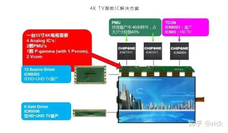
In high-definition televisions or vehicle display solutions, each screen requires a TCON chip. If the screen size increases, the demand for Driver ICs increases significantly. As shown in the figure below, 12 Source Drivers and 8 Gate Drivers are required, along with two PMUs (Power Management Chips) and three Vcom (Voltage Calibration Chips).
What has been discussed above pertains to displays; mobile phones are slightly different. In mobile phones, due to the concentration of various chip functions, the CPU/GPU and other chips equivalent to a computer’s main unit are all integrated into the Application Processor (AP), and the DDIC is also a chip that integrates all functions. Therefore, after information comes out from the AP, it will directly enter the DDIC through the MIPI DSI interface, and the DDIC can directly control the TFT without needing so many interfaces.
The above content introduces the main principles of displays, and next, we will explore the interface technologies between the AP and the display.
4. Display Interface Origins
To transmit display data from the SOC main chip to the display and complete the display, two major types of display interface technologies are required. One is the display interface from the CDC SOC to the TCON, and the other is from TCON to Gates/Sources. The latter is mainly implemented internally by the display manufacturers. The former requires more consideration, as it needs to be compatible with different SOCs, and their choice of display interface technology affects the input standards of the TCON.
Although this article mainly discusses vehicle display interfaces, the historical origins of these display interface technologies are primarily based on two major application scenarios: televisions or personal computers. Therefore, we will first review the development of digital video interface technologies, omitting those that are not relevant to the vehicle environment.
-
· LVDS:
Originally proposed by National Semiconductor (later acquired by Texas Instruments), based on LVDS (Low-Voltage Differential Signaling) technology, it converts parallel digital video signals into serial transmission. Each pair of LVDS differential signal lines transmits 7 bits of data. To transmit RGB666, four pairs of LVDS differential lines are needed. The transmission interface standards based on LVDS technology include OpenLDI, FPD-Link, DP (Display Port)/eDP, etc.;
-
· TMDS:
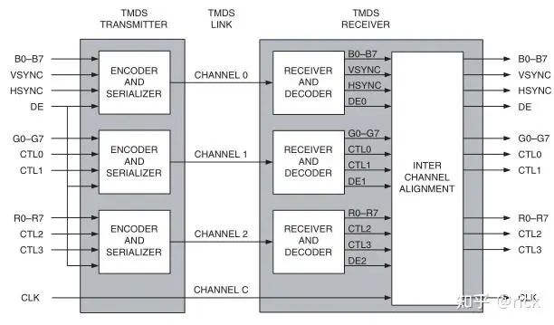
Originally developed by Silicon Image (now acquired by Lattice Semiconductor), the TMDS (Transition-Minimized Differential Signaling) technology solution is somewhat similar to LVDS at the physical layer, but completely different in communication protocol. It uses IBM’s 8b/10b encoding method to reduce the occurrence of errors and support longer cable lengths. When transmitting RGB888 image signals, it first serializes an 8-bit parallel signal (R/G/B components are 8/8/8 bits) into a 10-bit output, and then at the receiving end, it deserializes it back to 8 bits.
The first 8 bits of TMDS data are encoded, the 9th bit indicates the encoding method, and the 10th bit is for DC balancing.
One TMDS signal channel transmits 8 bits of data, requiring three TMDS signal channels to transmit R’G’B’ data, plus an additional clock channel. Each channel is also a pair of differential signal lines.
Transmission interface standards based on TMDS include DVI, HDMI, DFP, etc.
-
· MIPI DSI:
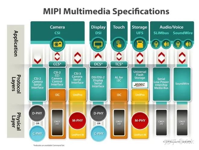
Unlike LVDS or TMDS, MIPI DSI is mainly used for display interfaces in mobile devices such as smartphones. MIPI stands for Mobile Industry Processor Interface Alliance, which was established in 2003 by ARM, Intel, Nokia, Samsung, STMicroelectronics, and Texas Instruments as a global open organization aimed at developing interface standards for the mobile ecosystem. After more than a decade of development, there are now over 250 member companies worldwide, and with the development of the mobile ecosystem, MIPI standards have entered fields such as artificial intelligence, the Internet of Things, virtual and augmented reality, automotive, cameras, industrial electronics, and medical facilities.
MIPI separates the physical standards of the interface from its transmission protocols. Currently, MIPI specifies three physical standards: M-PHY, D-PHY, and C-PHY. M-PHY is traditionally used for high-speed data transmission between chips, while D-PHY is used to connect cameras and display screens to the main chip set. Later, MIPI released the C-PHY standard, which serves the same purpose as D-PHY and can be considered an upgrade of the D-PHY standard.
MIPI DSI (Display Serial Interface) is a serial interface used in display technology. It sends pixel information or commands to peripheral devices (essentially LCD displays) in a serial manner and reads status information or pixel information from peripheral devices. During transmission, it has its own communication protocol, including data packet format and error detection mechanisms.
-
· Summary
Based on the brief introduction above, we can summarize the origins of digital video interface technologies applicable in vehicle environments as shown in the figure below:
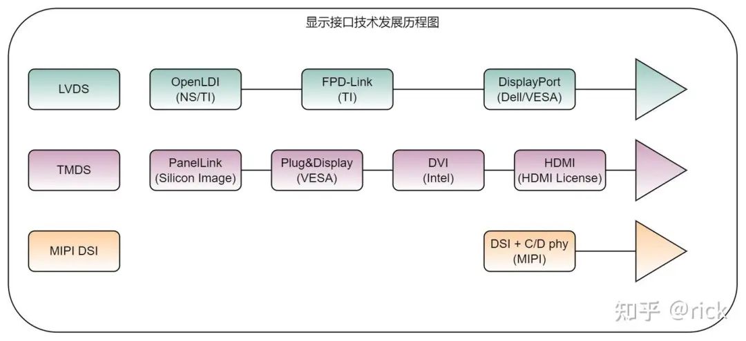
The specifications of the digital video interface for display systems are:
HDCP: High-bandwidth Digital Content Protection. EDID: Extended Display Identification Data. DDC: Display Data Channel. DMT: Display Monitor Timing. P&D: Plug and Display. DSC: Display Streaming Compression, a technology that compresses display data for transmission to save bandwidth, supporting high-definition video transmission with a maximum compression ratio of 3:1.
5. Interface Technologies
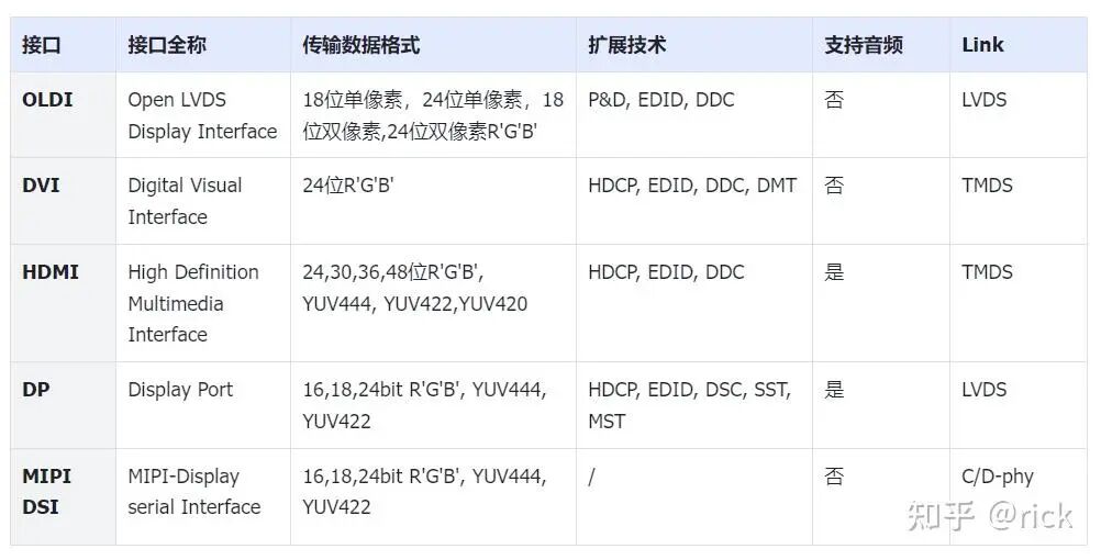
5.1 OLDI
When discussing video transmission interfaces, it is essential to understand video data formats. Generally, there are two methods to represent the color of each pixel. The first method uses three colors for each pixel, namely Red/Green/Blue, which are the three primary colors. If each color uses 8 bits (1 byte), then one pixel requires 3*8=24 bits of storage space. The second method uses YUV components. YUV is a type of true-color color space, and terms like Y’UV, YUV, YCbCr, YPbPr can all be referred to as YUV, with some overlap. “Y” represents luminance (Luminance or Luma), which is the grayscale value, while “U” and “V” represent chrominance (Chrominance or Chroma), which describes the color and saturation of the image, used to specify the color of the pixel. The storage space for YUV is usually smaller than that of RGB format, and under certain tolerable data loss (imperceptible to the human eye), RGB and YUV color formats can be converted to each other.
-
· Video Data Format:
18-bit single pixel R’G’B’: using 6-bit R’G’B’ values, R5~R0, G5~G0, B5~B0.
24-bit single pixel R’G’B’: using 8-bit R’G’B’ values, R7~R0, G7~G0, B7~B0.
18-bit dual pixel R’G’B’: representing two pixels as three 6-bit R’G’B’ values high/low pairs; RU5~RU0, GU5~GU0, BL5~BL0, RL5~RL0, GL5~GL0, BL5~BL0. Each high/low pair represents two pixels.
24-bit dual pixel R’G’B’: representing two pixels as three 8-bit R’G’B’ values high/low pairs; RU7~RU0, GU7~GU0, BL7~BL0, RL7~RL0, GL7~GL0, BL7~BL0. Each high/low pair represents two pixels.
-
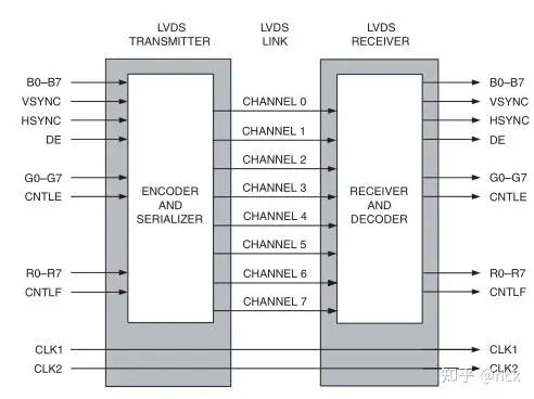
· OLDI Transmission
OpenLDI, the LVDS chain uses 8 pairs of serial data lines (A0~A7) and two sampling clock lines (CLK1 and CLK2). The actual serial data lines used depend on the pixel format, with a serial data rate of 7 times the sampling clock frequency. The CLK2 signal is used in dual pixel mode for backward compatibility with the FDP chain (a high-speed digital video interface) at the receiving end.
When transmitting 18-bit single pixel R’G’B’, the OpenLDI serial lines A0~A2 are used for transmission.
When transmitting 24-bit single pixel R’G’B’, the OpenLDI serial lines A0~A3 are used for transmission.
When transmitting 18-bit dual pixel R’G’B’, the OpenLDI serial lines A0~A2, A4~A6 are used for transmission.
When transmitting 24-bit dual pixel R’G’B’, the OpenLDI serial lines A0~A7 are used for transmission.
The LVDS chain supports video sampling rates and timings of 32.5~160 MHz.
As shown in the figure below, this is a schematic of the OpenLDI LVDS chain:
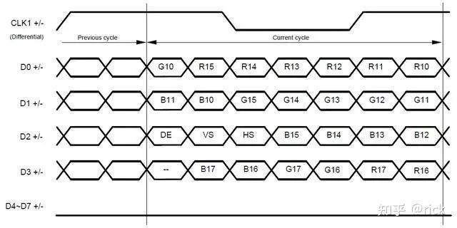
When transmitting display data, OLDI actually transmits 7 bits of data for each pair of differential lines, so within one clock cycle, 4 pairs of differential lines can transmit 28 bits of data, which includes 24 bits of data and 3 bits of control signals. As shown in the figure, D0+/- ~ D2+/- transmits RGB666+DE+VS+HS, while D3+/- transmits the remaining 6 bits of RGB. Therefore, 3 pairs of differential lines can transmit 18 bits of RGB666, and 4 pairs can transmit RGB888.
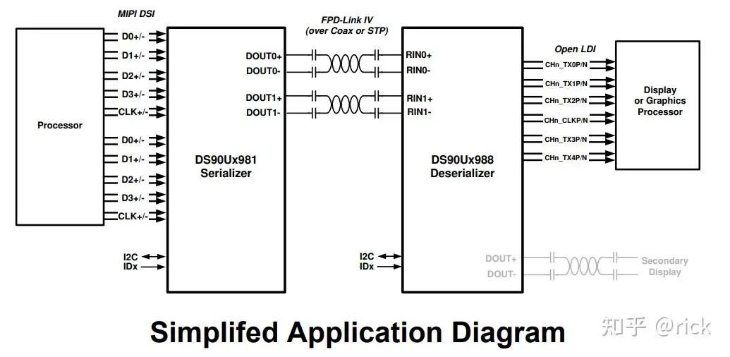
In practical use, TI’s FPD-link can support long-distance transmission of video data, performing deserialization at the de-serializer end to output RGB format data. This data is then transmitted to the display via the OLDI interface. At this point, the display’s TCON chip also uses the OLDI interface to input data.
5.2 HDMI
HDMI is developed based on TMDS technology, and it is somewhat similar to LVDS at the physical layer, also using differential pairs to transmit high-speed data signals. However, its encoding method differs from LVDS, primarily using IBM’s 8b10b encoding method.
The figure below illustrates the transmission architecture of HDMI:
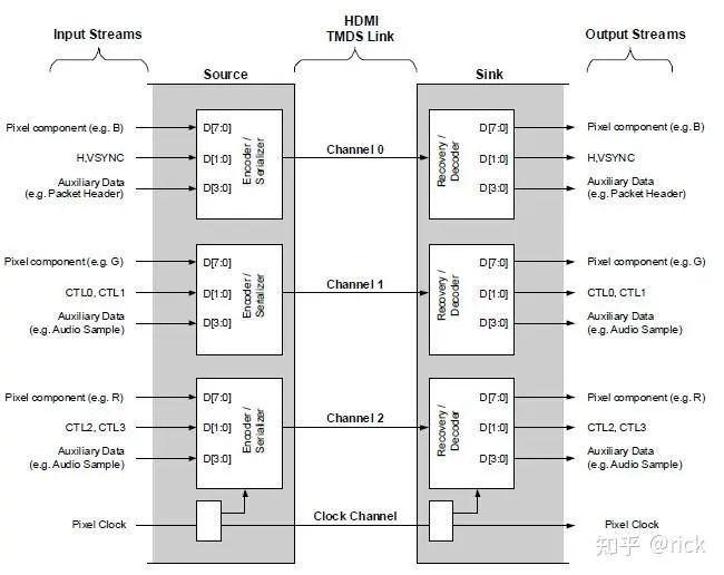
8-bit data at the source is converted to 10-bit data after passing through the TMDS encoder, and then serialized for output; at the sink end, it is first restored to 10-bit data and then decoded back to 8-bit source data through the TMDS decoder.
-
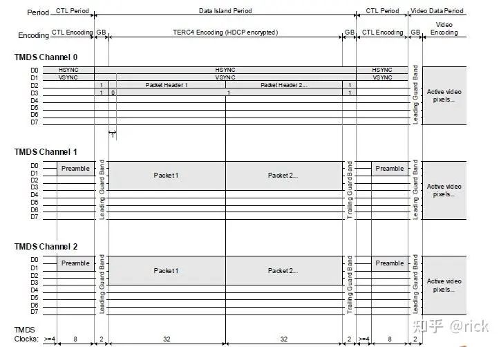
· Data Transmission Protocol
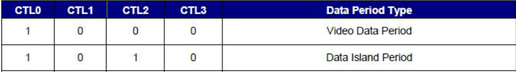
1. HDMI uses one Clock line and three data lines for transmission. The Clock signal line transmits the Pixel synchronization clock signal. On the data lines, a total of four types of signal can be transmitted:2. Preamble (control information), mainly used to control whether the subsequent transmitted data is Data Island or Video Data. In the figure, Preamble refers to CTL0, CTL1, CTL2, CTL3. They occupy D[1:0] channels of channel 1 and channel 2, totaling 4 bits;3. Data Island (data packets), various types of packet information, including audio data packets, image information packets, etc. In the figure, they occupy D[3:0] of three channels, totaling 10 bits of data input. For example, Channel 0’s D[3:2] is used to transmit Packet Header. Channel 1 and Channel 2’s D[3:0] are used to transmit Auxiliary Data packets, such as audio data, image resolution and format information, etc.;4. Video Data (video information), pixel data for video, HDMI can transmit pixel data in both RGB and YUV formats. In the figure, they occupy D[7:0] of three channels, totaling 24 bits of data input;5. Hsync and Vsync are transmitted through D[1:0] of channel 0:
If the transmitted data is Video Data and the format is RGB, it will occupy all 24 bits of input from the three channels, with Channel 0[7:0] used for B, Channel 1[7:0] for G, and Channel 2[7:0] for R.
If the transmitted data is Data Island, it will occupy 10 bits of input from the three channels, with Channel 0[3:2] used for Data Island Header (packet header), and Channel 1[0:3] and Channel 2[0:3] used for Data Island Content (packet data).
If the transmitted data is Preamble, it will occupy 4 bits of input from channels 1 and 2, with Channel 1[1:0] and Channel 2[1:0] being CTL0, CTL1, CTL2, CTL3, used to determine whether the subsequent input is Video Data or Data Island.
For Hsync and VSync, they will occupy two bits of input from Channel 0, with Channel 0[0] for Hsync and Channel 0[1] for Vsync.
-
· Transmission Cycle
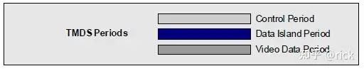
HDMI’s TMDS data transmission can be divided into three transmission cycles:
-
1. During the Control Period, Hsync and Vsync are transmitted, and at the end of this period, Preamble is transmitted.
-
2. During the Data Island Period, Data Island (data packets) is transmitted, along with Hsync and Vsync.
-
3. During the Video Data Period, Video Data (pixel data) is transmitted.
The overall cycle of a frame is as follows:
The transitions between the three transmission cycles are as follows:
-
· Effective Transmission Bandwidth
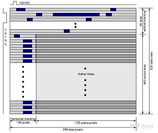
According to the above description, the effective data transmitted by HDMI is less than the high-speed transmission bandwidth provided by the physical layer. In addition to the loss from 8b10b encoding, there is also the loss caused by the switching of the three transmission cycles. The effective image transmission bandwidth is: (720*480) / (858*525) * (8/10) = 345600/450450 * 8/10 = 61.3%;
5.3 DP/eDP
DisplayPort is a digital video interface standard developed by a consortium of PC and chip manufacturers and standardized by VESA (Video Electronics Standards Association). This interface is royalty-free and does not require certification, primarily used for connecting video sources to displays and also supports audio, USB, and other forms of data.This interface is designed to replace traditional VGA, DVI, and FPD-Link (LVDS) interfaces. Through active or passive adapters, this interface can be compatible with traditional interfaces (such as HDMI and DVI).
eDP (Embedded DisplayPort) protocol is an extension of the DP (Display Port) application in embedded architecture and protocols, so the eDP protocol is fully compatible with the DP protocol. Compared to DVI/HDMI, eDP has high bandwidth, good integration, and simple related product design, and this interface has been widely used in laptops, tablets, smartphones, and other fields with integrated display panels and image processors.
The system architecture of DP is as follows:
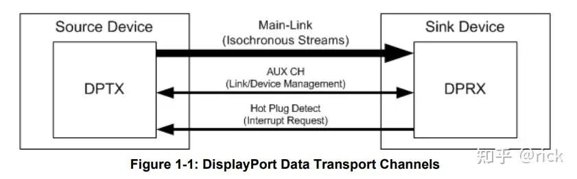
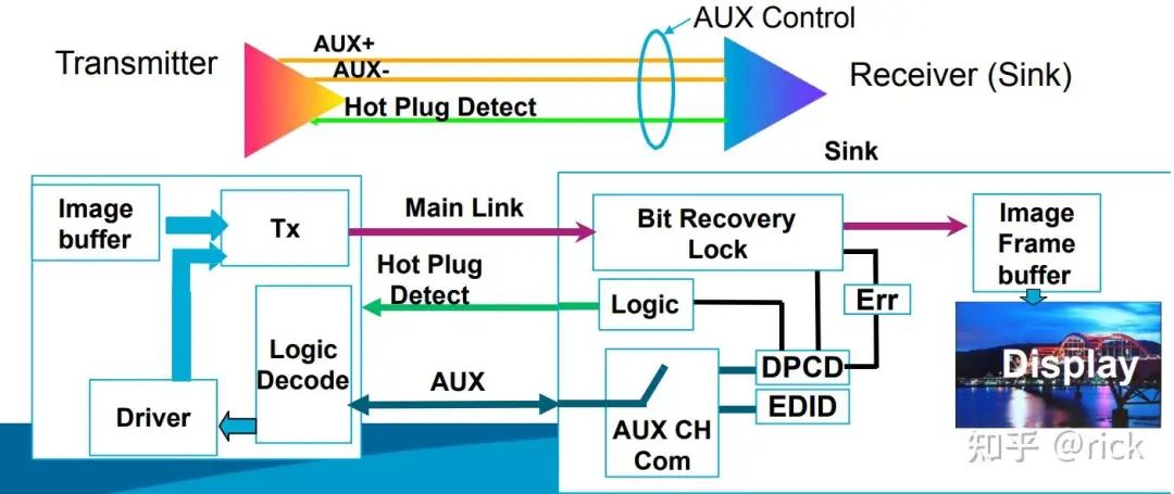
DP consists of a Source end and a Sink end. The Source end is the image sending end, typically a device like a GPU that generates images. The Sink end is the playback end, typically a display device.
The system architecture of eDP is as follows:
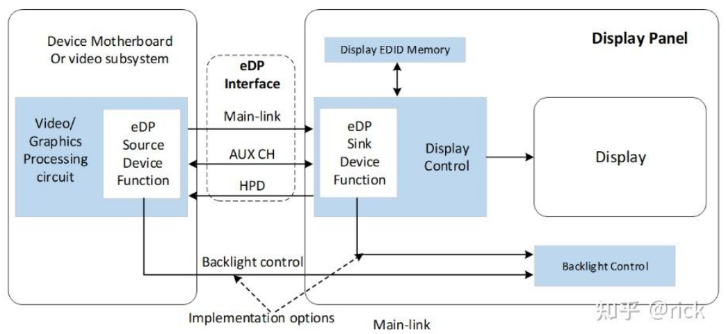
The differences between DP and eDP are:
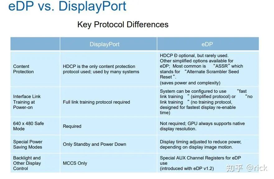
The main differences between DP and eDP are that DP can transmit video data over long distances (>2m) via wired cables, while eDP is generally used for board-level, internal video data transmission. Additionally, due to the external interface, DP generally requires digital content protection functionality, i.e., HDCP; whereas for eDP, since the interface is not exposed, HDCP functionality is optional and rarely used.
From the system architecture diagram, it can be seen that both DP and eDP need to include three main components:
-
1. Main-Link:
The main link is a unidirectional, high-bandwidth, low-latency channel used to transmit synchronized data streams such as uncompressed video and audio. Note that the Main-Link can be 1 Lane, 2 Lanes, or 4 Lanes. Each lane consists of a pair of differential signal lines.
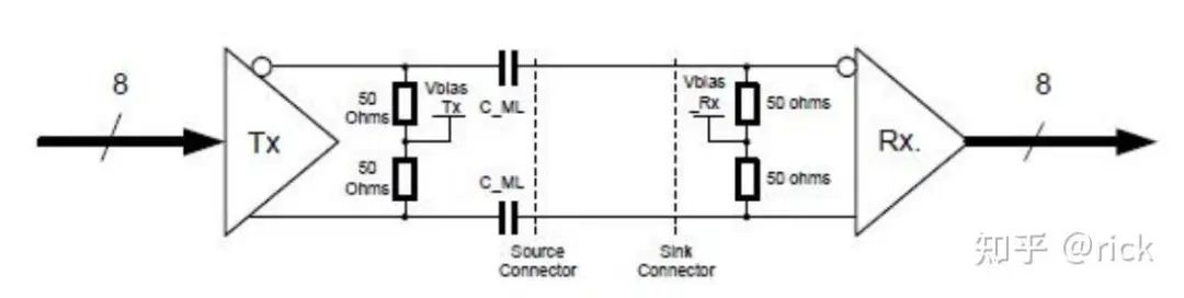
The data transmitted on each Lane is encoded using 8b10b encoding, meaning that 8 bits of data at the TX end are expanded to 10 bits, embedding clock information. At the RX end, it is decoded back to the original 8-bit data. This design allows for better electromagnetic compatibility in long-distance transmission. Additionally, the data Lane transmission already includes clock information, eliminating the need for an additional clock signal line.
Due to this feature of the Main link, before starting DP transmission or when detecting errors during transmission, a Link training process must be initiated. This training is primarily to compensate for signal loss on connectors and cables to ensure error-free data transmission.
The training process will be conducted via the AUX CH. When the Source detects the HPD signal, it recognizes that a sink has been inserted and will initiate DP training.
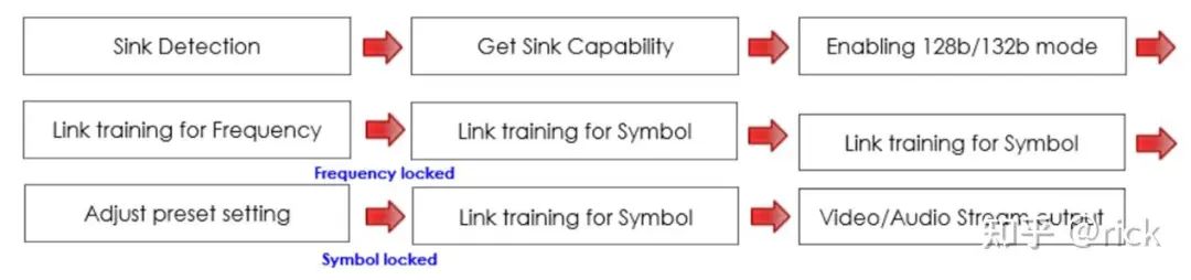
Note: In the DP2.0 protocol, the 8b/10b encoding has been changed to 128b/132b encoding, providing higher bandwidth utilization.
The figure below is a schematic diagram of the Link training process for DP2.0:
2. AUX CH:
The Aux channel is a half-duplex bidirectional data channel used for link management and device control.
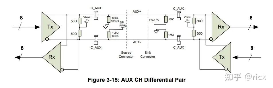
In the Aux Channel, the transmitted signal is Manchester encoded with embedded clock signals, thus eliminating the need for a separate clock signal line. As shown in the figure, the first clock cycle detects a falling edge (from H to L), indicating a signal of 1; the second clock cycle detects a rising edge (from L to H), indicating a signal of 0, and so on.
3. HPD:
Hot Plug Detect, a separate signal line used to send an interrupt from the Sink end to the Source end, notifying that the Sink device has been inserted. The figure below is a schematic diagram of a DP system:
DP’s transmission protocol
From the layered architecture of DP transmission, the Link layer provides three services: Isochronous Transport Services, AUX CH Device Services, and AUX CH Link Services. Isochronous Transport Services mainly package and fill the transmitted audio and video data, AUX CH Device Services manage the source and receiving devices, such as reading EDID information. AUX CH Link Services maintain and configure the link, ensuring correct establishment of the link, synchronization of clocks between the receiving and sending ends, and accurate data transmission on the main link.
These three services operate under the direction of the Stream Policy Maker and Link Policy Maker, controlled by the Policy Maker.
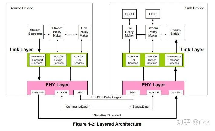
The PHY layer is mainly responsible for sending/receiving data.
In the receiving device, there is a display port configuration register, which contains configuration data (DPCD) that describes the functionality of DPRX, similar to how EDID describes the functionality of the receiving display. Link and Stream Policy Makers manage Link and Stream respectively.
In the data transmission of the Main link, the data is packaged and sent in the following format:
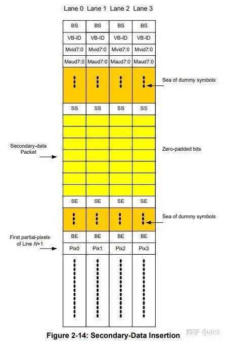
It is important to note that SDP stands for Secondary Data Packet. In the DP protocol, SDP is used to transmit the following information:(1) CEA-861-F INFOFRAME SDP(2) Audio_Stream SDP(3) Audio_TimeStamp SDP
Audio data will be sent from the SDP data packet. The DP protocol documentation provides detailed descriptions of the types of SDP and various transmission packet structures. If interested, you can refer to it; it will not be elaborated here.
The SD and SE signals transmit the SDP packets. After the BE and FS signals, the actual pixel data transmission begins until the FE signal ends. Here, FS stands for Fill Start, and FE stands for Fill End.
DP’s transmission bandwidth
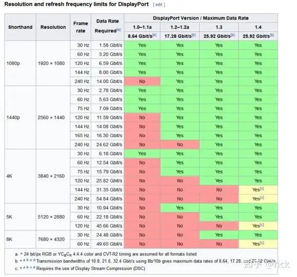
DP can transmit 16, 18, 24-bit R’G’B’, YUV444, YUV422, and other formats of video stream signals. It also uses 8b/10b encoding format. Therefore, when calculating the bandwidth rate required by the display, these factors must be considered. Additionally, the impact of blanking must be taken into account, calculated using Htotal*Vtotal. The table below shows the theoretical physical bandwidth and effective bandwidth specifications for different versions of DP:

For a 4K@60fps video transmission requirement, if using 24-bit RGB format transmission, the required bandwidth is:
-
· Resolution: 3840×2160 (Htotal=3920, Vtotal=2222)
-
· Refresh Rate: 60Hz
-
· Color Depth: 8 bits
-
· Color Format: RGB 24-bit (RGB: 8 times 3, YC422: 8 times 2, YC420: 8 times 1.5)
Multiplying these four related parameters together gives the required bandwidth:3920 * 2222 * 60 * 8 * 3 = 12,542,745,600 (12.543Gbps)
If DP cannot provide sufficient bandwidth, 24-bit RGB can be converted to YUV422 color format for transmission, in which case the required bandwidth becomes:3920 * 2222 * 60 * 8 * 2 = 8,361,830,400 (8.362Gbps)
By consulting the table below, you can find the DP effective bandwidth that meets the requirements. That is, DP v1.2 and above, 4-lane transmission can meet the 4K@60fps requirement. If DP only supports up to V1.0, then YUV422 format transmission must be used.
5.4 DSI
DSI is a high-speed serial interface defined by the MIPI Alliance, located between mobile application processors and display modules. MIPI stands for Mobile Industry Processor Interface, which is evidently designed for mobile application processors and is widely used in smartphones, tablets, and other products. As Qualcomm and other original mobile chip manufacturers enter the smart cockpit market, it is now necessary to consider how to support the DSI interface in automotive cockpits. The most common usage scenario is to output DSI signals from the AP, which are then input to the display via OLDI or eDP through a serial de-serializer.
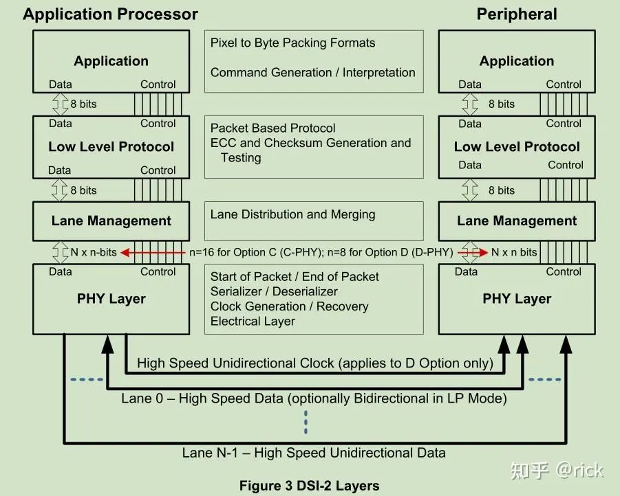
DSI Layered Structure
DSI is divided into four layers, corresponding to D-PHY, DSI, DCS specifications, and the layered structure diagram is as follows:
-
· PHY defines the transmission medium, input/output circuits, and clock and signal mechanisms.
-
· Lane Management layer: sends and collects data streams to each lane.
-
· Low Level Protocol layer: defines how to frame and parse data, as well as error detection, etc.
-
· Application layer: describes high-level encoding and parsing of data streams.
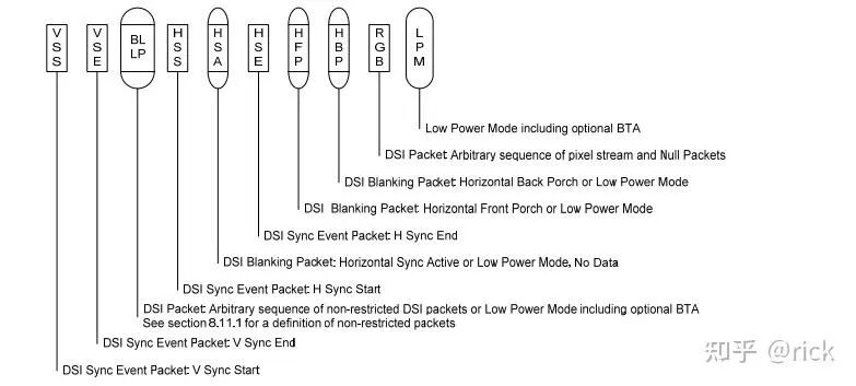
Command and Video Modes
DSI-compatible peripherals support Command or Video operation modes, with the choice of mode determined by the architecture of the peripheral.
Command mode refers to sending commands and data to a controller with a display buffer. The host indirectly controls the peripheral through commands. Command mode uses a bidirectional interface.
Video mode refers to transmitting real-time pixel streams from the host to the peripheral. This mode can only be used for high-speed transmission. To reduce complexity and save costs, systems that only use Video mode may have only a single-direction data path.
DSI System Block Diagram
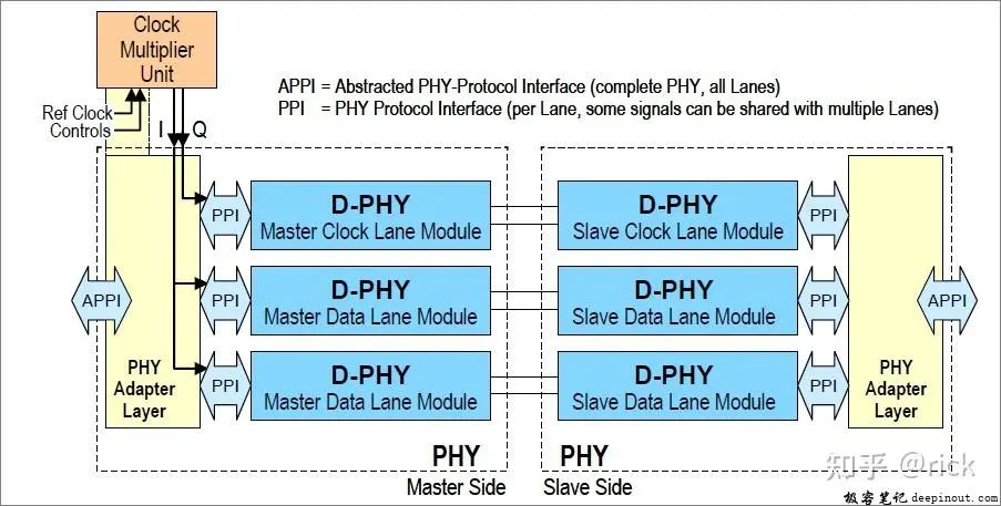
The above architecture mainly describes the transmission connection method of the MIPI-DSI D-PHY interface used internally in mobile devices (if it is C-PHY, the physical layer architecture differs from D-PHY). A DSI port has one pair of clock transmission lines and 2 or 4 pairs of data transmission lines, referred to as 2-lane or 4-lane. As shown in the figure, the D-PHY structure shows the connection of one clock lane and two pairs of data lanes.
MIPI DSI transmits data in a frame structure, with each frame being either a fixed 4 bytes (short frame) or a variable-length frame (long frame). Each pair of data lanes starts with a SoT (Start of Transmission) byte and ends with an EoT (End of Transmission) byte, then transmits byte by byte. For example, with 2 pairs of data lanes, the transmission method is shown in the figure below:

The long frame structure transmitted by DSI is shown in the figure below:
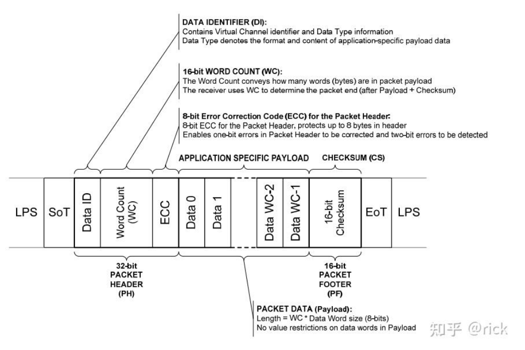
Packet data consists of multiple RGB data packets, and each RGB data packet is shown in the figure below:
6. Display Applications
6.1 Instrument Cluster
The instrument cluster is the only display device in the vehicle that needs to consider functional safety (Functional Safety, Fusa). In the era of traditional fuel vehicles, the information provided by the dashboard mainly includes: vehicle speed, engine speed, fuel level information, light status information, various safety alert status icons, etc. Among these, safety alert status icons need to meet ASIL-B level functional safety requirements. These safety alert icons are commonly referred to as “telltales”.
To ensure that the “telltales” meet the ASIL-B level Fusa standards, relevant processing must be performed on the display system of the smart cockpit SOC. According to the ISO-26262 specification requirements, the entire chain for processing telltale events must meet ASIL-B standards. This includes the initial source of safety information, the channel for transmitting safety information to the SOC, how the SOC generates the corresponding alert icons, how the SOC displays the corresponding alert icons, and how to compare and detect whether the icons match the original safety information without errors or omissions. This is particularly important for the instrument cluster. This includes both hardware devices and software systems. For example, does the operating system that generates telltale information meet ASIL-B level requirements?
6.2 Central Control Screen
The central control screen, also known as the Instrument Central Screen (ICS), has become an essential device in the era of smart vehicles. It is the most important entry point for users to control all vehicle devices, understand the vehicle’s status, and engage in entertainment, serving as a necessary carrier for the “second space”.
Technically, the central control screen does not have special requirements; generally, it needs to meet the following conditions:
Screen Size: The central control screen comes in various sizes, including 8, 10, 11.3, 12.3, 12.8, 14, 15, 17, and 17.7 inches. Its resolution generally requires to be above 1080P. For example, the central control screen of the BMW i4 and iX is 14.9 inches with a resolution of 2880*1080 and a pixel density of 206 ppi; similarly, the NIO ES8 has an 11.3-inch central LCD screen with a resolution of 1400*1600 and a pixel density of 188 ppi. Regarding refresh rates, at least 60Hz is required, and 90Hz should soon be achievable for mass production. Only under such conditions of resolution, refresh rate, and screen size can the vehicle entertainment system achieve an experience similar to that of consumer electronics like smartphones and tablets.
Touch Screen: In the era of smart vehicles, many physical buttons have been eliminated, and their functions have been integrated into the central control screen. This requires good touch capabilities to enhance user experience. It is hard to imagine a user waiting a long time for feedback when using the touch function on the central control screen. Technically, the central control screen must provide responsive touch functionality, and the smart cockpit SOC must provide sufficiently fast interrupt response and processing capabilities.
Long-Distance Transmission: Inside the vehicle, the distance between the central control screen and the smart cockpit SOC can sometimes exceed 10 meters. If sufficient data processing capability (resolution * refresh rate) is to be ensured while meeting the requirements of the vehicle environment, the layout of the SerDes transmission cable must be considered.
Integration of IC and ICS: Currently, some new energy vehicles have begun to gradually eliminate the IC instrument display screen. They integrate the relevant display content into the central control screen, designating a specific area to display relevant information. It is important to note how the telltale function is integrated into the ICS screen and how to ensure that the telltale icons displayed on the ICS screen meet ASIL-B functionality.
6.3 Head-Up Display (HUD)
The HUD (Heads Up Display) system, as a comprehensive electronic display device, can project vehicle information such as speed, fuel consumption, engine speed, navigation, etc., onto the windshield or other display media for the driver to view, thereby reducing safety hazards caused by the driver looking down or diverting their gaze.
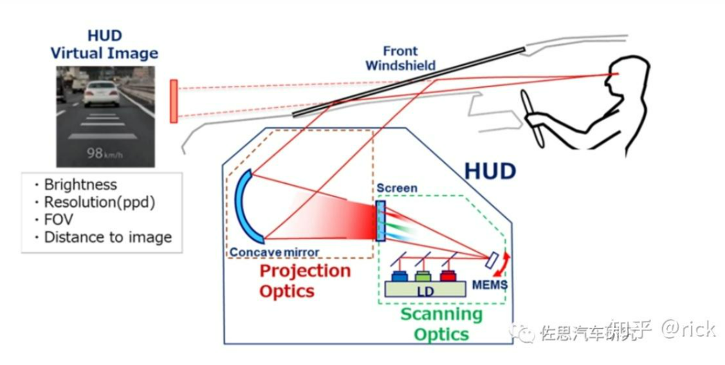
The principle is to enlarge the image information displayed by the image source through a lens or reflection system and then reflect it to the driver’s eye activity area, i.e., the eye box, at a certain distance in front of the windshield, forming a virtual image, thus presenting instrument and central control information more intuitively in front of the driver’s eyes.
According to the imaging method and display content of HUD, current vehicle HUDs can be divided into the following three categories:
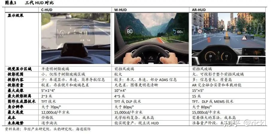
C-HUD (Combiner HUD): C-HUD is commonly found in the aftermarket, where a semi-transparent resin board is added above the vehicle dashboard, serving as the projection medium. Through a semi-reflective curved mirror, the displayed image from the image source is enlarged and projected a virtual image ahead. C-HUD has flexible layout but its drawbacks mainly include a small field of view, small virtual image size, and short projection distance, along with noticeable ghosting effects, leading to an overall poor experience, which is technically difficult to resolve and may gradually be phased out.
W-HUD (Windshield HUD): This can directly project images onto the vehicle’s windshield, supporting a larger imaging area and longer projection distance. The disadvantage of W-HUD is that the windshield is usually a curved reflective mirror, and W-HUD must adapt high-precision curved mirrors according to the size and curvature of the windshield, resulting in relatively high costs, mainly applied in mid-to-high-end models, and is currently being popularized in mid-to-low-end models.
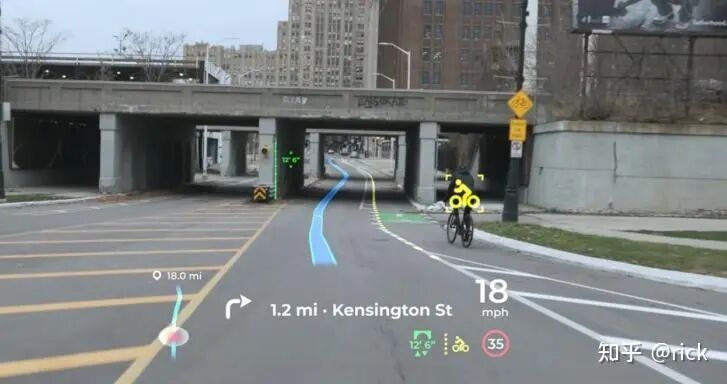
AR-HUD (Augmented Reality HUD): Like W-HUD, it uses the windshield as the imaging medium, but AR-HUD applies augmented projection surface technology, with a field of view (FOV) greater than 10° and an imaging distance (VID) greater than 7 meters, allowing for richer information presentation. AR-HUD requires modeling and parsing the road conditions ahead through intelligent driving sensors (cameras, radars, etc.) to obtain the position, distance, size, and other elements of objects, and then accurately project the HUD display information onto the corresponding position. AR-HUD can highly integrate projected information with traffic environments, such as lane lines fitting during driving, alignment with obstacles/hazards ahead, lane departure warnings, etc.
AR-HUD has outstanding display effects and is an important component of intelligent driving and smart cockpits.
Currently, the drawbacks of AR-HUD include its large size, making it difficult to install in vehicles. Additionally, the technology is not yet mature, and its display effects and information acquisition accuracy still need improvement.
Comparison of Three Generations of HUDs
Structure of HUD
In terms of structural composition, HUD mainly consists of three parts: imaging, optical projection, and software.
Imaging:
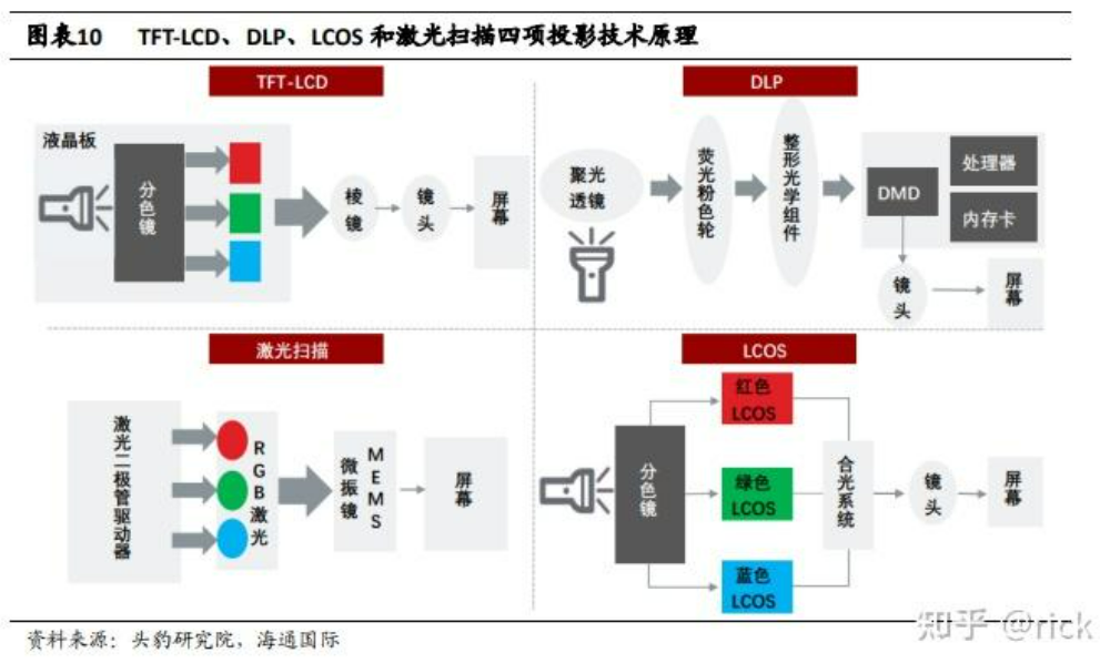
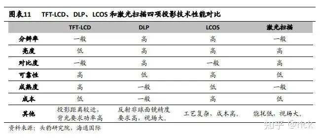
The main imaging component of HUD is the image source, referred to as PGU (Picture Generation Unit). Currently, mainstream PGU solutions are divided into four types: TFT, DLP, LCOS, and LBS.
· TFT, or TFT-LCD, uses liquid crystal display panels for transmission imaging. This solution is the earliest developed projection solution in the industry and is mature. Its principle is to use liquid crystal display panels for transmission imaging, illuminated by backlight, but the liquid crystal blocks most of the light, resulting in insufficient brightness and generating a lot of heat.
· DLP, which stands for Digital Light Processing, is a patented technology by Texas Instruments. It projects light through a DMD (Digital Micromirror Device) that integrates hundreds of thousands of micro-mirrors. Compared to TFT imaging technology, DLP does not require liquid crystal polarizers but uses DMD reflective projection, reducing brightness loss. Images produced by DLP technology have high resolution, high contrast, and realistic imaging, but the cost is relatively high.
· LCOS (Liquid Crystal on Silicon) is a type of matrix liquid crystal display device based on reflection mode, which is relatively small in size. This matrix is manufactured using CMOS technology on silicon chips. LCOS technology projects light through color separation mirrors onto three LCOS panels, then combines the light to form an image. LCOS has advantages in resolution, brightness, and color.
· LBS, or Laser Beam Scanning, is a projection display technology that combines RGB laser modules with Micro-Electro-Mechanical Systems (MEMS). It uses lasers as the light source, projecting through MEMS micro-mirrors, offering advantages such as small components, low energy consumption, high brightness, and large field of view, but the cost is very high, and laser diodes are sensitive to temperature, unable to meet the 85°C operating requirement, so laser scanning projection has not yet been widely applied in vehicle HUDs.
Optical Projection
Optical projection enlarges the light emitted by the PGU and projects it onto the windshield, which is the two reflection parts in the AR HUD schematic above—a fixed reflective mirror and a free-form reflective mirror. Currently, the size of the entire HUD mainly comes from this optical projection part.
Software
The software part mainly includes AR generators, in-vehicle maps, navigation systems, voice systems, etc. Among them, the AR generator (ARCreater) is a complete set of AR display hardware and software solutions that integrates data and spatial coordinates to render virtual information onto real scenes, forming a display effect that merges virtual and real information. Specifically, the AR generator needs to integrate the following data:
· Road element recognition data, generated through convolutional neural networks for image depth learning, to create recognition models that scan and identify the area of interest (ROI) in the real scene ahead, obtaining spatial coordinates for lane lines, vehicles, pedestrians, non-motorized vehicles, traffic signs, traffic lights, and other road objects;
· AR navigation information, which includes route information such as turns, distances, times, and navigation instructions such as traffic conditions, lane information at intersections, along with POIs and speed camera information;
· Other information, such as vehicle operation information like speed, RPM, water temperature, voltage, tire pressure monitoring, blind spot alerts, ACC, etc.; multimedia information such as incoming calls, Bluetooth, FM, etc.
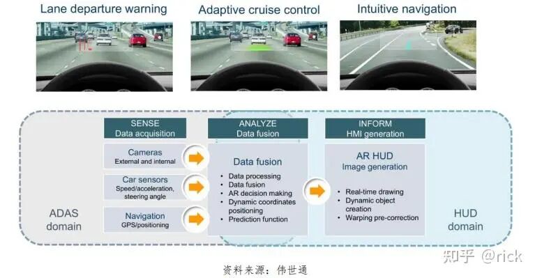
AR HUD must integrate information from navigation and ADAS systems, while also considering precise positioning, timestamps, 3D rendering, UI/UX, and predictive capabilities to provide drivers with more accurate and effective prompt information.
*Disclaimer: The source of this article is Zhihu, and the copyright belongs to the original author.If there is any infringement, please contact Luko for verification and deletion. The content of the article represents the author’s personal views, and Luko’s reprint is only to convey a different perspective, not representing Luko’s endorsement or support of that view. Comments and discussions are welcome in the comment section.