
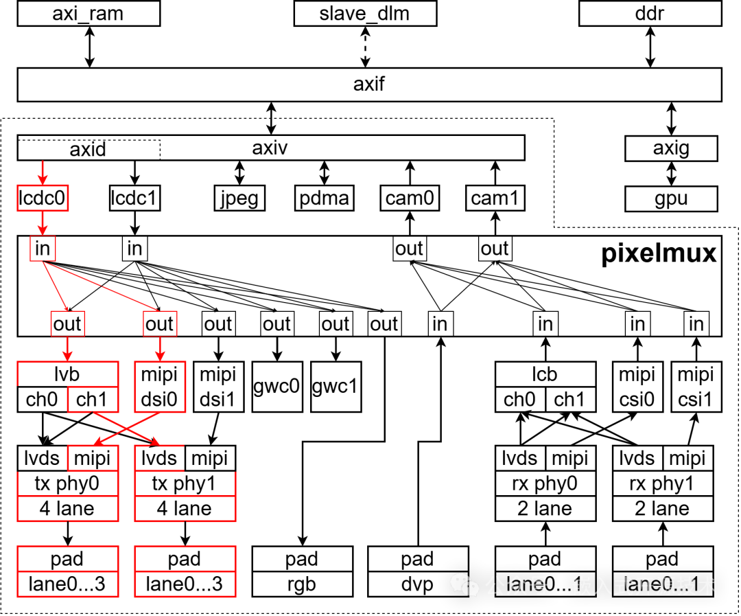
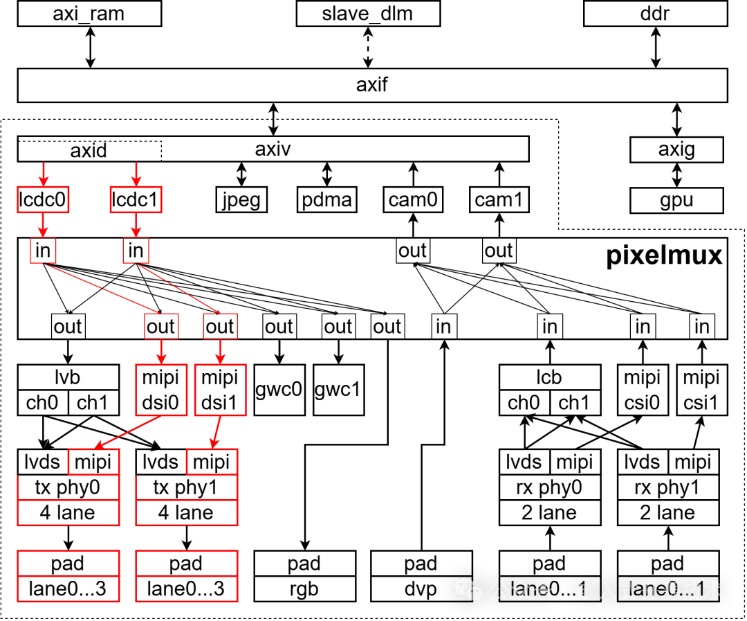
The display subsystem of the HPM6800 series features a rich set of graphical peripherals. The above diagram clearly illustrates the functional structure of the entire display subsystem, allowing us to easily understand the data flow of pixel interfaces and the interconnection relationships between each peripheral. The display subsystem mainly consists of a memory access bus, PIXELMUX, display IPs, camera IPs, and image processing IPs.
Memory Access Bus
The memory access bus is used for graphical IPs within the display subsystem to access memory. Each graphical IP has its own AXI memory access interface, which allows access to memory devices, such as reading and writing pixel data.
- AXIF Bus Matrix
AXIF stands for AXI Fast, and through the AXIF bus, almost all types of memory devices on the SoC can be accessed, such as AXI RAM, DDR, and slave DLM. The most commonly used memory type for the HPM6800 is DDR due to its large capacity and high speed. Graphical IPs have high memory access requirements, so DDR memory can meet almost all usage scenarios.
- AXIV Bus Matrix
AXIV stands for AXI Vision, and this bus mainly connects various graphical IPs, including LCDC, CAM, JPEG, and PDMA. AXIV can access memory devices through AXIF, while these graphical IPs access memory devices via AXIV. As shown in the diagram, CAM, JPEG, and PDMA access memory through the AXIV clock domain, while LCDC accesses memory through the AXID clock domain. In simple terms, the clock speed of the AXI bus for LCDC is AXID, while the clock speed for CAM, JPEG, and PDMA is AXIV. AXID is just one port of the AXIV bus matrix, representing an asynchronous clock domain, which is different from the AXIV bus bridge clock. Generally, the core clock of graphical IPs is synchronized with the AXI clock. In other words, the clock for the LCDC IP is AXID, while the clocks for the other three IPs are AXIV. Clocking is very important for IPs, and we will highlight this when introducing each IP later.
- AXIG Bus Bridge
AXIG stands for AXI GPU, and this bus bridge is mainly used for the connection between the GPU and AXIF, allowing the GPU to access various types of memory devices through AXIG and AXIF.
PIXELMUX
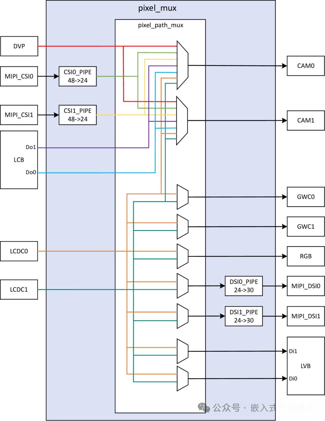
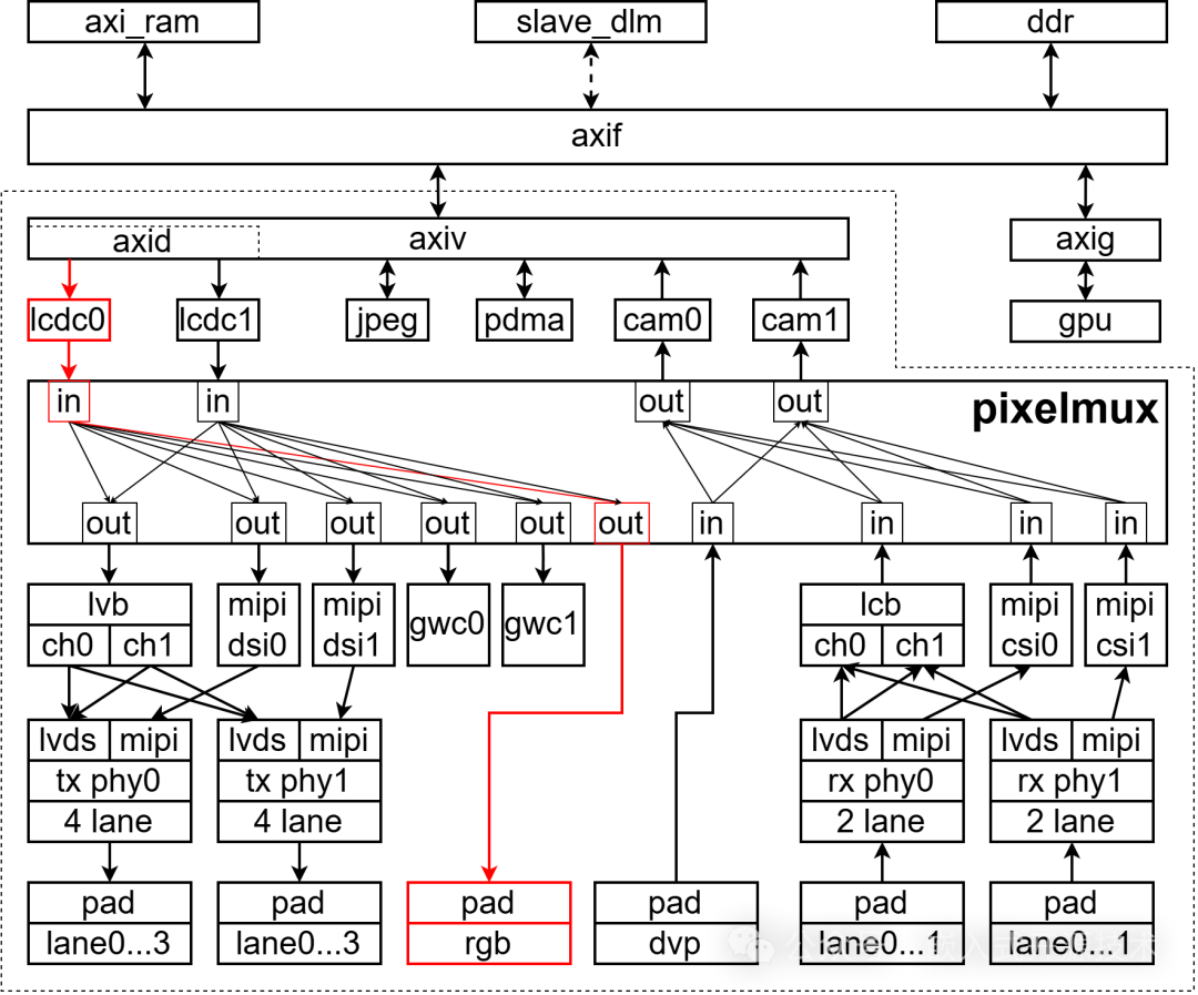
PIXELMUX is responsible for the interconnection of image data between various image modules in the VIS subsystem and also provides miscellaneous configuration functions for some IPs, such as configuring the LVDS PHY and pixel conversion configurations during interconnection between IPs. From the above diagram, we can clearly see the direction of pixel data flow. For example, if I want to display through LCDC0 and RGB interface, I first need to establish the pixel link through PIXELMUX. As shown in the diagram below.
- In/Out Ports
On PIXELMUX, whether it is an in port or an out port, there will be a corresponding graphical IP, meaning that the graphical IP will be connected to PIXELMUX through the in or out port. Each pixel will flow in through the in port, pass through PIXELMUX, and flow out from one or more out ports. This process may change the pixel format or keep it unchanged. Whether the pixel format changes depends on whether the pixel formats of the IPs corresponding to the in and out ports are consistent.
- Pixel Format Conversion
As mentioned above, when pixels flow from the in port to the out port, the data and pixel format may change.
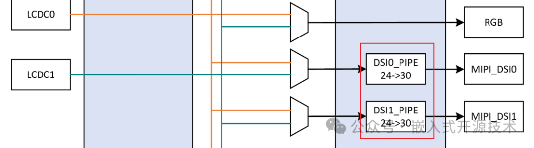
For example, if we display through the path <span>lcdc0->mipi_dsi0</span>, the pixels output by LCDC0 will enter the in port of PIXELMUX, and after passing through PIXELMUX, they will enter the mipi_dsi0 from the out port of PIXELMUX. At this point, pixel format conversion needs to be enabled because the pixel format output by LCDC may not be the format required by mipi_dsi. At this time, it is necessary to convert the pixel format output by LCDC to the format required by mipi_dsi. We will discuss the required pixel format for mipi_dsi in related articles. Here, we just want to illustrate that PIXELMUX has the function of pixel format conversion, not just a pixel interconnection switch.
Dual Screen Same/Different Display
The advanced display subsystem can flexibly circulate pixels through the PIXELMUX peripheral, which also enables the possibility of dual screen same display and dual screen different display. As mentioned earlier, the in port of PIXELMUX can correspond to one or more out ports, meaning that the pixels coming in from the in port can be distributed to multiple out ports, thus achieving dual screen same display.
- Dual Screen Same Display
As the name suggests, dual screen same display means that the images on the two displays are exactly the same. In theory, we can achieve, for example, two MIPI screens displaying the same content, or two single-channel LVDS screens displaying the same content, or one LVDS and one MIPI screen displaying the same content. However, it is not possible to display MIPI and RGB together or LVDS and RGB together, not because this display subsystem does not support it, but because the pins of the HPM6800 MCU do not support it, as the pins for RGB, MIPI, and LVDS are multiplexed. Additionally, it is important to note that for dual screen same display, the resolutions of the two screens must be the same, as both screens receive the same pixels output from LCDC. Below is a diagram showing one LVDS and one MIPI achieving dual screen same display through PIXELMUX.
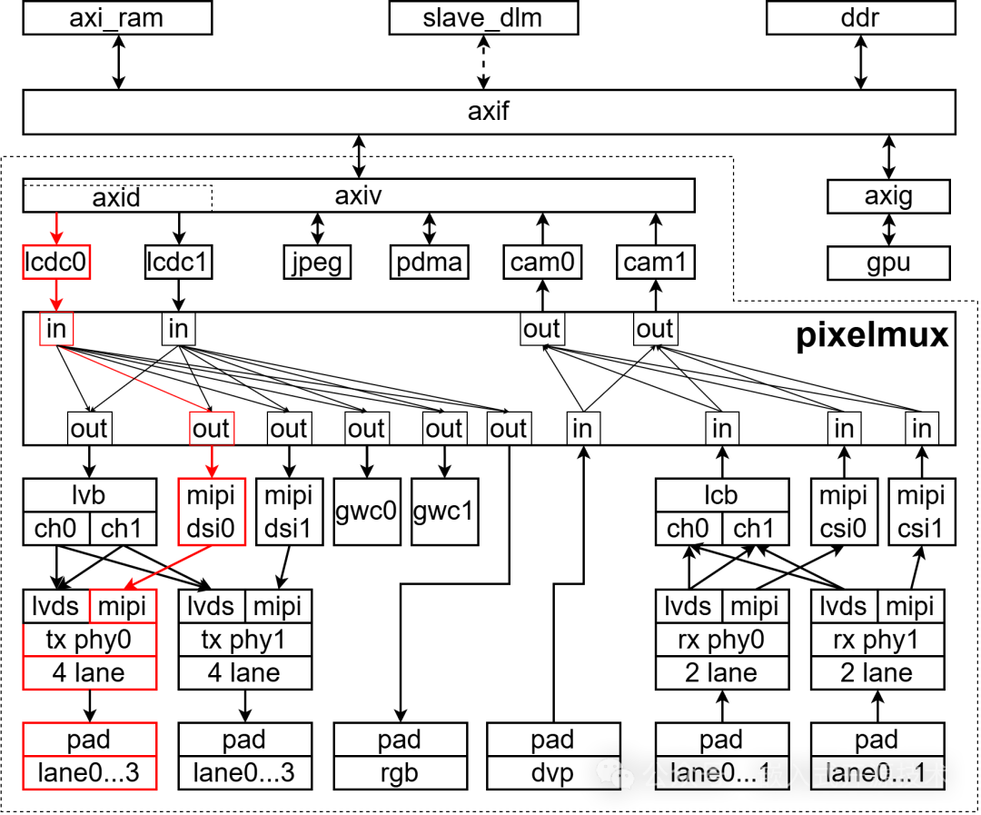
- Dual Screen Different Display
The HPM6800 features two LCDC controllers, which enables dual screen different display. With two LCDC controllers, we can drive two completely independent displays. For example, we can have two MIPI screens displaying different content, or two single LVDS screens displaying different content, or one LVDS and one MIPI screen displaying different content. However, it is also not possible to display MIPI and RGB differently or LVDS and RGB differently. Below is a diagram showing two MIPI screens achieving dual screen different display through PIXELMUX.
Future Plans
Based on this article, we will subsequently explain the functions, programming models, and usage methods of each peripheral. Understanding the block diagram at the beginning of this article is especially important for mastering the advanced display subsystem, as it provides a global perspective of the subsystem and the interconnection relationships between each peripheral. This diagram will be referenced multiple times in the upcoming articles. For those interested in the advanced display subsystem, it is essential to deeply understand this diagram. Of course, if there are any inaccuracies, please feel free to point them out to the official or developers.