Follow us for free updates on avionics news.

Abstract
The Remote Data Interface Unit (RDIU) is responsible for protocol conversion in aircraft, connecting various subsystems such as remote sensors and actuators to the aircraft’s backbone network, forming a mixed onboard network configuration. Existing RDIU protocol conversion technologies face issues such as incomplete participation of protocols, long conversion cycles, and poor data real-time performance. This paper proposes the protocol conversion principles for UART, ARINC429, and ARINC825 bus protocols used by remote data devices and the AFDX global data bus protocol of the aircraft, completing the hardware architecture design for protocol conversion and using the hardware description language Verilog HDL for detailed design. Simulation test results indicate that the design can correctly perform conversions between multiple protocols, and the implementation of the hardware architecture improves data processing efficiency.
Keywords
RDIU; protocol conversion; mixed onboard network; hardware architecture

1 Introduction
Avionics systems are particularly important as the control center of civil aircraft, and integrated modular avionics systems (IMA) are now widely used in large civil aircraft. In IMA, the avionics full-duplex switched Ethernet (AFDX) serves as the backbone network, forming the framework for integrated avionics. However, remote data interface units (RDIUs) are still required in aircraft to achieve mutual conversion between various protocols and AFDX signals. RDIUs are distributed throughout the aircraft, centralizing the processing of dispersed remote signals collected by sensors and transmitting data from the application host to remote actuators after processing. These subsystems use various communication protocol buses as secondary buses connected to the core aviation data network, forming a mixed onboard network configuration.
Research on RDIU protocol conversion functions has been conducted both domestically and internationally. Liu Liansheng et al. implemented a bus conversion interface design between AFDX and ARINC429 protocols using soft-core processors and HI-8583 chips. N. Rejeb et al. studied how to communicate in a hybrid architecture of AFDX/CAN, proposing methods for intercommunication between two types of signals. However, the above studies only performed simple repackaging of data, which does not conform to the application information format of resident software. Duan Weize used a PowerPC+FPGA structure for RDIU design, achieving mutual conversion between multiple protocols and AFDX based on embedded technology. This research is limited by the general architecture of the processor, interrupt handling mechanisms, and operating system scheduling, resulting in poor real-time performance and uncertainty in the protocol conversion process. Furthermore, most research works lack specific designs for certain interface protocol conversions and do not provide RDIU designs capable of simultaneously completing mutual conversions between multiple protocols and AFDX.
This paper analyzes the protocol conversion rules and implementations for the three main protocols involved in the conversion (UART, ARINC429, ARINC825) and AFDX, proposing a hardware architecture to complete the RDIU protocol conversion work. The protocol conversion process is centralized at the data link layer using hardware coding, and the packaging and unpacking functions of AFDX data frames are also added to this architecture, further improving data processing efficiency. A highly configurable RDIU multi-protocol conversion system that meets the real-time requirements of onboard networks is designed, achieving bidirectional protocol conversion between general serial protocol data and AFDX data frames. It should be noted that this paper mainly focuses on the design of the conversion architecture and does not involve the electrical characteristics of protocol transmission, targeting the digital signal processing of data frames that conform to protocol formats.
2 Protocol Conversion Principle Design
There are various protocol interface subsystems on the aircraft, which brings many inconveniences to the overall interconnection of avionics systems, preventing high resource sharing and optimal overall performance. There are three solutions to this problem: 1) unify the bus interface protocols of all avionics devices; 2) enable the upper management system to support multiple bus interface protocols simultaneously; 3) determine one bus interface protocol as the backbone network of the aircraft and connect other interface protocols to the backbone network through protocol conversion. The first two solutions currently face multiple issues such as high research difficulty, high development costs, and maintenance difficulties due to system over-coupling, so the third protocol conversion method is commonly adopted to solve such problems. For avionics systems, the IMA architecture is currently widely used, and RDIU can complete protocol conversion work within this architecture. The principle diagram of the IMA architecture is shown in Figure 1.
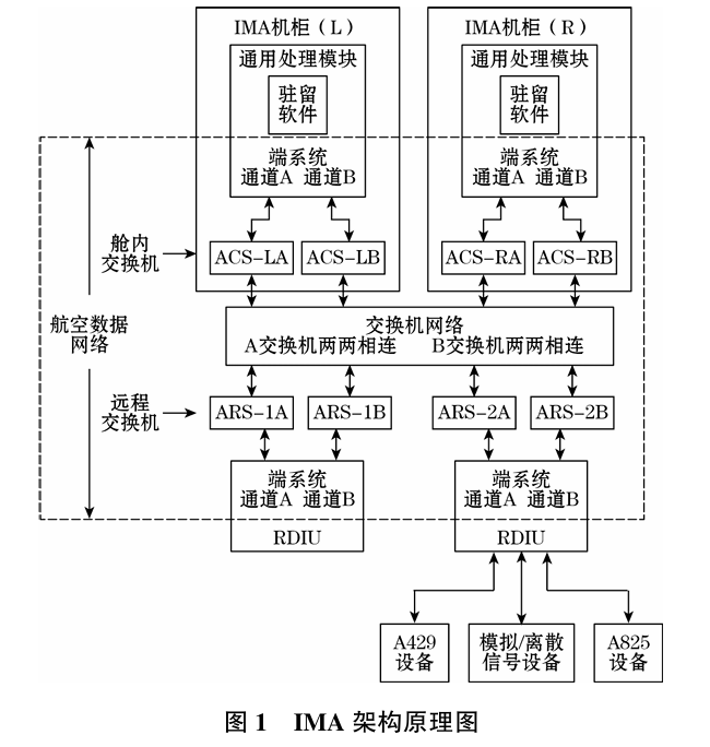
The IMA architecture consists of IMA cabinets, aviation data networks, RDIUs, and remote signal devices. Each IMA cabinet is equipped with a general processing module with resident software, connected to the AFDX bus as the backbone aviation data network through end systems and switches, to complete the transmission and reception of data signals from various systems on the backbone network. RDIUs are distributed throughout the aircraft to collect remote data signals and complete protocol conversion with the aircraft’s global data bus. The remote data signals that need to be converted to AFDX mainly include the following three types: analog/discrete signals, ARINC429, and ARINC825. For analog/discrete signals, they can be converted to digital signal formats through analog-to-digital conversion and digital signal processing. Considering the transmission of this digital signal, the widely used and mature asynchronous serial UART protocol in civil aviation is selected for data transmission. The following introduces the application information format of AFDX and the bidirectional protocol conversion rules between UART, ARINC429, ARINC825 signal data, and AFDX signal data frames.
2.1 AFDX Application Information Format
The AFDX bus protocol is developed based on commercial Ethernet, improving traditional Ethernet for aircraft bus communication. It is a star network that meets the interconnection communication requirements of integrated avionics systems for large and medium-sized aircraft, becoming the recommended choice for the next generation of aviation data networks. Its data frame structure and application information format are shown in Figure 2.
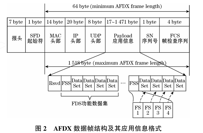
The AFDX data frame consists of a header, start symbol, MAC header, IP header, UDP header, Payload application information, sequence number, and frame check sequence. The Payload application information, as the key part of protocol conversion, has the following characteristics: the first word of the application information is a reserved word (Rsvd); it provides the concept of functional data set (functional dataset, FDS) to encapsulate data, where one FDS consists of one functional status set (functional status set, FSS) and 1 to 4 data sets (dataset, DS).
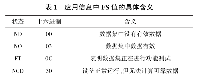
The functional status set FSS is a 32-bit field composed of four 8-bit functional status (FS) fields. The nth functional status (FS) field is used to indicate the status of the nth data set (n≤4); the functional status FS indicates the status of the corresponding data set DS, which is an 8-bit enumeration field defining four statuses, with specific meanings as shown in Table 1; the data set DS is the actual transmitted data, and its length must be a multiple of 32 bits.
2.2 Remote Data and AFDX Protocol Conversion Principles
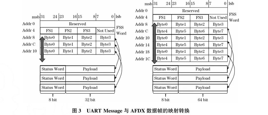
For UARTMessage with a Payload of 32 bits, its DS has a fixed size of 4 bytes; for UARTMessage with a Payload of 64 bits, its DS has a fixed size of 8 bytes. This is because if the status field corresponding to a DS is marked as invalid, the entire DS is marked as invalid, so fixing the length of each channel’s DS can improve efficiency and reduce the cost of data errors.
When converting UART data, if the status word information is NO or FT, it is packed into FS, and the corresponding DS is filled with the data segment of the UART data packet; if the status word information is NCD, it is packed into FS, and the corresponding DS is filled with 0; if the status word information is ND or other, the data packet is discarded. When converting to UART data, if FS is NO or FT, the FS and corresponding DS are packed into a UART data packet and sent through the UART port; otherwise, it is discarded.
2.2.2 ARINC429
ARINC429 specifies the digital information transmission requirements between avionics devices and related systems, supporting full-duplex communication, with a pair of differential signal lines for transmission and reception interfaces, using bipolar return-to-zero three-state code modulation for data transmission, characterized by simple structure, stable performance, and strong anti-interference. The transmission rates of ARINC429 are divided into low speed (12.5 kbit/s) and high speed (100 kbit/s), with each data frame consisting of 1 bit parity bit P, 2 bit status bits SSM, 19 bit data bits DATA, 2 bit source/destination identifier SDI, and 8 bit data word identifier.
2.2.1 UART
UART is an asynchronous serial communication method, and UART serial communication adopts full-duplex communication, allowing simultaneous transmission and reception operations, using two data lines for sending and receiving data. Two UART data packet formats are defined, consisting of a 1-byte status word and data segment, where the status word has the same values and meanings as FS, and the data segment widths are 32 bits and 64 bits, with the mapping conversion diagram of AFDX data frames shown in Figure 3.
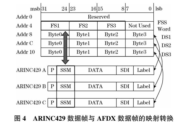
Defining the ARINC429 protocol conversion process, each DS contains only one ARINC429 data. When converting ARINC429 data, the parity bit is first checked; if it passes the check, the next step is determined based on its SSM; otherwise, the data is discarded. For data that passes the check, if the SSM mapped FS is NO or FT, the corresponding value is filled in FS, and the ARINC429 data is packed into the corresponding DS; if the SSM mapped FS is NCD, the corresponding value is filled in FS, and the corresponding DS is filled with 0; if the SSM mapped FS is ND, the data is discarded.
When converting to ARINC429 data, if FS is NO or FT, the corresponding DS is checked for parity, and the newly calculated parity bit is filled back into the data, which is then sent as an ARINC429 data packet through the ARINC429 port; otherwise, it is discarded.
2.2.3 ARINC825
The ARINC825 standard is based on the existing Controller Area Network (CAN) standard, standardizing its use in aircraft. The ARINC825 bus is widely used in internal networks of subsystems such as power, lighting, and cockpit control panels. The ARINC825 bus adopts half-duplex transmission, inheriting the extended frame format of CAN, using a 29-bit identifier (ID) and supporting priority transmission of abnormal event messages, normal communication messages, service messages, and test maintenance messages through logical channel division. It supports multiple transmission rates of 125 kbit/s, 250 kbit/s, 500 kbit/s, and 1 Mbit/s, with the data frame format and mapping conversion diagram of AFDX data frames shown in Figure 5.
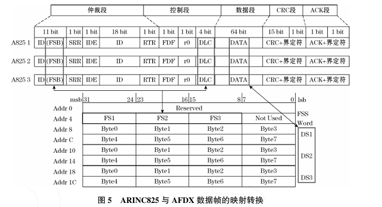
Similar to CAN data frames, ARINC825 data frames consist of arbitration segments, control segments, data segments, CRC segments, and ACK segments, in addition to using frame start and end segments to indicate the beginning and end of the frame. In this design, the length of the ARINC825 data segment published by the application host is specified as 64 bits, defining that each DS in the protocol conversion process contains only one ARINC825 data frame’s data segment. When converting ARINC825 data, if the {FSB, DLC} mapped FS is NO or FT, the corresponding value is filled in FS, and the ARINC825 data is packed into the corresponding DS; if the {FSB, DLC} mapped FS is NCD, the corresponding value is filled in FS, and the corresponding DS is filled with 0; if the {FSB, DLC} mapped FS is ND, the data is discarded. When converting to ARINC825 data, if FS is NO or FT, the FS mapped {FSB, DLC} and corresponding DS are packed into an ARINC825 data packet and sent through the ARINC825 port; otherwise, it is discarded.
3 Hardware Architecture of the Protocol Converter Design
3.1 Overall Architecture Design
The hardware architecture for protocol conversion is shown in Figure 6.
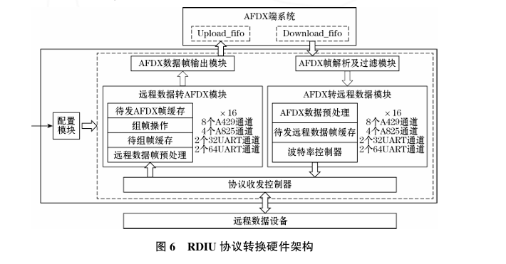
The protocol conversion part includes configuration modules, protocol transceiver controllers, remote data to AFDX modules, AFDX to remote data modules, AFDX data frame output modules, and AFDX frame parsing and filtering modules. The remote data to AFDX module consists of remote data frame preprocessing, framing cache, framing operations, and AFDX frame cache for transmission; the AFDX to remote data module consists of AFDX data preprocessing, remote data frame cache for transmission, and baud rate controllers. All ARINC825 channels can accept ID numbers, acceptable ID wildcard masks, and ID numbers when sending ARINC825 serial signals.
3.2 Detailed Hardware Circuit Design
The overall architecture of the protocol conversion part consists of six modules, specifying the functions of each module and the data processing tasks to be completed. Programs are written in hardware description language Verilog HDL based on the functions of each module, mapping them to specific digital hardware circuits.
3.2.1 Configuration Module
The configuration module is used to configure the entire protocol conversion process, receiving configuration data through a fixed 921600 bit/s UART interface. A configuration data packet has a width of 40 bits, consisting of 8 bits for the address and 32 bits for the write data. The configuration module writes the received data into the corresponding register addresses to set protocol conversion parameters. Configuration parameters include the transmission baud rate of each channel interface, the reception mode (periodic reception and event-triggered reception) when converting device data signals to AFDX data frames, the reception period (5~320 ms), and the number of events triggering reception (1~64 channel data words), as well as the IP destination address fields, UDP destination address, MAC multicast address virtual link number, and the types of ARINC429 data words received by all ARINC429 channels (BCD, BNR, discrete). When receiving serial data, it will be processed according to the interface protocol and complete serial-to-parallel conversion, forming data packets that conform to the protocol conversion process. For ARINC429 signals, the bit numbers corresponding to the ARINC429 data words in the serial data transmission order are 0~7, 8~31, placing each received ARINC429 data word into a 32-bit data packet for transmission to the next module; for ARINC825 signals, after identifying and receiving ARINC825 signals, it filters out ARINC825 CAN messages that do not match the configured ID and those that fail CRC checks, placing the remaining valid messages’ FSB and DLC into the high 5 bits of a 69-bit data packet and placing Data into the low 64 bits, sending the completed 69-bit data packet to the next module; for UART signals, after identifying the start and stop bits, it extracts the data transmitted by UART, with the UART serial data transmission order corresponding to the UART parallel data bit numbers 0~7, placing each received byte sequentially from the high bit into a 40-bit/72-bit data packet and sending it to the next module. When sending serial data, the serial output is performed according to the data packet received by the protocol transceiver controller and the data validity indicator, with the received data packet format being the same as its sending format, and the sending process of each protocol signal is the reverse of its receiving process.
3.2.2 Protocol Transceiver Controller
The protocol transceiver controller integrates the protocol controllers of three types of remote data buses to receive protocol serial signals that conform to electrical characteristics after physical layer level conversion.
The architecture has three main functions: 1) Asynchronous serial UART configuration function for the system: there is a UART interface in the architecture, and each remote signal channel has a register address allocation table set according to its characteristics. Configuration information will be input into the architecture’s module registers through this interface, including protocol transceiver control, protocol conversion rules, packaging and unpacking information, and multiple registers. 2) Remote signal data frame to AFDX data frame: receiving serial digital signal data frames from remote data devices after level conversion, the protocol transceiver controller completes serial-to-parallel conversion, inputting the specified format data packets into the remote data to AFDX module, where data mapping and framing operations are completed to convert into AFDX data frame format, which is finally controlled and written into the end system’s Upload_fifo by the AFDX data frame output module. 3) AFDX data frame to remote signal data frame: receiving AFDX data frames from the end system’s Download_fifo, filtering out the data frames that meet the requirements after AFDX frame parsing, inputting them into the AFDX to remote data module, where data mapping and exception handling are completed to obtain remote signal data frames that can be recognized and serially output by the protocol transceiver controller, and then the baud rate controller determines the interval for sending the data frame to the protocol transceiver controller, sending it out in the format of serial digital signals.
3.2.3 Remote Data to AFDX Data Frame Module
This module receives various protocol data packets sent by the protocol transceiver controller, divided into 16 channels, with each channel corresponding to one of the 16 receiving channels of the protocol transceiver controller.
When each channel receives a data packet, it will preprocess the remote data frame, first checking the content of each received data packet. For A429 data, it will check whether its parity bit is correct; for UART data, it will check whether its status word value is within the enumeration range; for A825 CAN data, it will check whether its DLC is within the enumeration range. After checking, the abnormal or correct data packets will undergo FS mapping, discarding those mapped to 0x00 and setting the DS corresponding to those mapped to 0x30 to 32’b0/64’b0; finally, the valid data in the received data will be converted into the form of 8bit FS + 32bit/64bit DS, forming 40bit/72bit data packets stored in the channel’s framing cache. The maximum configurable event trigger condition is to receive 64 data packets, and it is also specified that the number of data packets received under periodic triggering does not exceed 64, so the framing cache is set to a width of 40bit/72bit and a depth of 64 FIFO. The data entering the framing cache is monitored, and when the number of data packets in the framing cache reaches the event trigger condition or periodic trigger condition, a framing start signal is sent to the framing module, and framing operations begin: first, according to the values in the configuration register, the MAC header, IP header, and UDP header are completed and stored in the AFDX frame cache, where the MAC source address and IP source address are the attributes of the RDIU, and the UDP source address is set to 16 different values based on the data from different receiving channels. Additionally, to ensure data alignment, two empty bytes are added after the header information as padding to align the 32bit data bits, and then, according to the conversion rules, the data in the framing cache is converted into the application information Payload of the AFDX data frame and sent to the AFDX frame cache for transmission, which is implemented in FIFO form, with a fixed width of 32bit. Since the data packets participating in the conversion do not exceed 64, and considering the length of each header information, the cache depth for the 32bit data word channel can be set to 128, and the cache depth for the 64bit data word channel can be set to 256.
3.2.4 AFDX Data Frame Output Module
This module is designed to select the channel from which to read data from the multi-channel AFDX frame cache, ultimately outputting it to the end system’s Upload_fifo. The module adopts a time-slice output method to improve the real-time performance and determinism of the entire architecture, outputting data from the AFDX frame cache of the 16 channels within the set time slice. If a framing completion signal is received from a certain channel, all data in that channel’s AFDX frame cache will be sent out in the next time slice.
When the main clock frequency is 50 MHz, each time slice can be set to 42 μs. For sending AFDX data frames of the 32bit channel, the maximum AFDX frame is 368 bytes: 4 bytes reserved + 4×(64/4) bytes FS bits + 64×4 bytes DS bits, plus 14 bytes MAC, 20 bytes IP, 8 bytes UDP header, and 2 bytes padding, totaling 368 bytes, which corresponds to 92 data packets in the 32bit FIFO (92×20ns=1.84μs); for sending AFDX data frames of the 64bit channel, the maximum AFDX frame is 624 bytes: 4 bytes reserved + 4×(64/4) bytes FS bits + 64×8 bytes DS bits, plus 14 bytes MAC, 20 bytes IP, 8 bytes UDP header, and 2 bytes padding, totaling 624 bytes, which corresponds to 156 data packets in the 32bit FIFO (156×20ns=3.12μs). Each 32bit channel is allocated a 2 μs time slice to send AFDX frames, and each 64bit channel is allocated a 3.5 μs time slice for sending AFDX frames, totaling 10 32bit channels + 6 64bit channels, plus a 1 μs idle time slice, so the total time slice can be set as: 2×10+3.5×6+1=42μs, indicating that the conversion process from remote data to AFDX data in this architecture will occur within 42 μs, and this time does not exceed 75% of the fastest trigger event time, ensuring that data congestion does not occur while guaranteeing the real-time output of data.
3.2.5 AFDX Frame Parsing and Filtering Module
This module mainly completes the unpacking and filtering of AFDX data frames, filtering out data packets that do not conform to the AFDX data frame format.
Receiving AFDX data frames composed of 32bit data packets output from Download_fifo, it performs frame parsing operations, parsing the MAC header, IP header, and UDP header, checking whether the MAC destination address, Ethernet protocol type, IP protocol number, IP header checksum, IP destination address, version number, time to live, protocol number, UDP destination address, and UDP checksum meet the reception conditions, filtering out frames that do not meet the conditions, and storing the MAC source address, IP source address, and UDP source address information into the corresponding registers of the target channel to send to the application host. It also completes channel selection based on the UDP destination address, sending the Payload in the AFDX frame to the corresponding channel of the next module.
3.2.6 AFDX Data Frame to Remote Data Module
This module receives the application information Payload data packets processed by the AFDX frame parsing and filtering module, divided into 16 channels, selecting channels according to the results of parsing the UDP destination address.
Each channel receives the unpacked and filtered application information Payload data and performs data preprocessing. According to the data format defined by different protocols and the values in the FS field, each FDS is converted into 1 to 4 remote data frame data packets. For ARINC429 data, during this process, the new parity bit calculation and replacement will also be completed, and then the preprocessed data will be packed into the corresponding protocol data packets, writing them into the remote data frame cache for transmission. Since the application host limits the application information Payload in an AFDX data frame to within 64 channel data words, this cache is set to a FIFO with a depth of 64. Finally, the baud rate controller sends the data packets in the cache to the protocol sending controller according to the sending baud rate configuration parameters in the configuration register, outputting these data frames as correct serial signals that conform to the remote data protocol format. Considering data congestion, when a certain channel is performing serial output, it will send a serial output flag signal to the frame parsing and filtering module, and when this signal is valid for a certain channel, the frame parsing operation for the AFDX data frame sent to that channel will not be performed.
4 Simulation Verification
To verify the correctness of the design, functional simulation was conducted on the hardware description language Verilog code that implements the functions of this system.
4.1 Remote Data to AFDX Data Frame
Taking the a channel of various types of remote signals as an example, data is first input to the configuration interface to configure the four channels involved in the work, with the reception mode set to event-triggered. Each channel will package four valid data packets into an AFDX data frame for transmission. Figure 7 shows the simulation results of converting remote data serial signals into AFDX data frames, where o_afdx_tx_dout and o_afdx_tx_valid represent the output value of the AFDX data frame and its valid signal, respectively. It can be seen that the design simultaneously processes multiple serial signals and outputs them as AFDX data frames upon reaching the trigger condition.
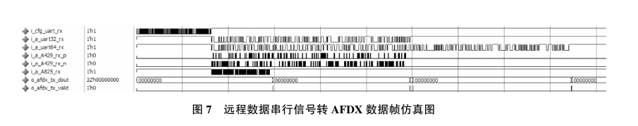
Figure 8 shows the A825 data and its converted AFDX data frame, with a total of 5 A825 data received, where a_A825_data is the received data segment, and a_A825_fsb and a_A825_dlc together represent the status of the A825 data, which will be mapped to the FS field of the AFDX data frame during conversion, and i_a_A825_rx is the received A825 serial data.
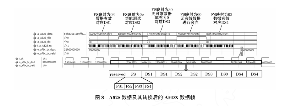
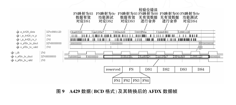
Figure 9 shows the A429 data (BCD format) and its converted AFDX data frame, with a total of 6 BCD format A429 data received, where a_A429_data is the sent A429 data, the 32nd bit is the parity bit, and the 31st and 30th bits are status bits used to indicate the status of the A429 data, which will be mapped to the FS field of the AFDX data frame during conversion, and i_a_A429_rx_p and i_a_A429_rx_n are the received A429 serial data.
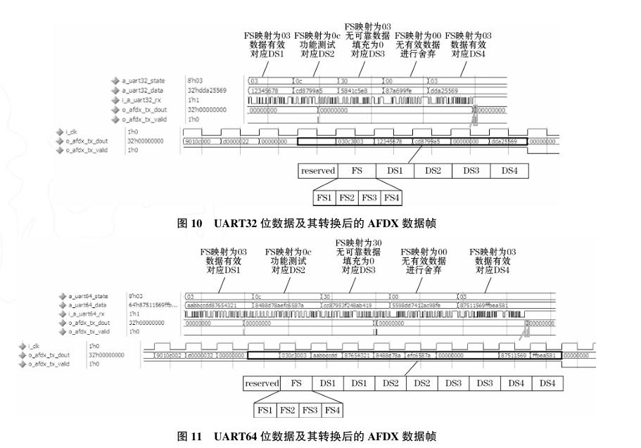
Figures 10 and 11 show the 32-bit UART data and 64-bit UART data and their converted AFDX data frames, with each channel receiving 5 UART data packets, where a_uart_data is the sent UART data, and a_uart_state is the status bit used to indicate the status of the UART data, which will be mapped to the FS field of the AFDX data frame during conversion, and i_a_uart_rx is the received UART serial data. The simulation diagrams show that the system can correctly receive the serial data input from remote devices at the set baud rate after configuration, correctly complete the mapping of the functional status word FS and the processing of the data set DS, and correctly send the AFDX data frames based on the reception mode and header information configuration.
4.2 AFDX Data Frame to Remote Data
Retaining the previous configuration, during the simulation, AFDX data frames that meet the requirements are simulated for sending, where i_afdx_rx_din is the received AFDX data frame, and i_afdx_rx_valid and i_afdx_rx_last are the valid signal and end signal of the AFDX data frame, respectively.
Figure 12 shows the A825 channel receiving the AFDX data frame and its converted serial data frame simulation diagram, receiving one AFDX data frame containing four A825 data, where o_a_A825_tx is the sent A825 data serial signal, and a_A825_txdata is the key data of the A825 data packet obtained after parsing the serial signal, where the high five bits are {fsb, dlc[3:0]}, indicating the status of the A825 data.
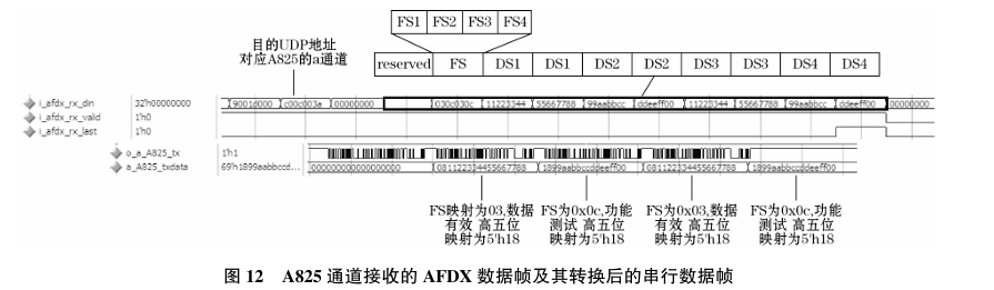
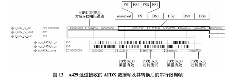
Figure 13 shows the A429 channel receiving the AFDX data frame and its converted serial data frame simulation diagram, receiving one AFDX data frame containing four A429 data, where o_a_A429_tx_p and o_a_A429_tx_n are the sent A429 data serial differential signals, and a_A429_txdata is the A429 data packet obtained after parsing the serial differential signal, where the highest bit is the parity bit, and the 31st and 30th bits are SSM bits used to indicate the status of the A429 data.
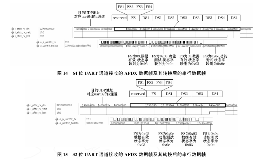
Figures 14 and 15 show the 64-bit UART channel and 32-bit UART channel receiving the AFDX data frame and its converted serial data frame simulation diagrams, receiving one AFDX data frame containing four UART data packets, where o_a_uart_tx is the sent UART data packet serial signal, and a_uart_txdata is the UART data packet obtained after parsing the serial signal, where the high eight bits are the status word indicating the status of the UART data packet. The simulation diagrams show that after receiving the AFDX data frame, the frame can be correctly parsed and filtered, and through the preprocessing conversion process, the application information Payload of the AFDX data frame is converted and mapped into remote data frames. Finally, the baud rate controller sends the remote data frames to the protocol transceiver controller based on the configured sending baud rate, allowing it to output correct serial signals that conform to the remote data protocol format.
5 Conclusion
This paper introduces three common types of remote data signals on aircraft, namely ARINC429, ARINC825, and UART signals, proposing the conversion principles and rules between these remote signals’ data frames and AFDX data frames, and designing a hardware processing architecture for RDIU protocol conversion. Simulation verification shows that it can parallelly complete bidirectional protocol conversion between multiple remote data and AFDX data frames. This paper adopts a hardware architecture for data processing to complete protocol conversion, unaffected by the interrupt and scheduling mechanisms of processors, and can achieve parallel processing, simultaneously completing protocol conversion for multiple channels and protocols, which is much faster than traditional software architectures, with low conversion latency, improving data processing efficiency and ensuring data real-time performance. Additionally, the architecture integrates protocol transceiver interface control functions and AFDX data frame packaging and unpacking functions, enhancing the design’s versatility and maximizing the advantages of the hardware architecture.
(This article is selected from “Instrumentation Technology and Sensors” by Jin Zhiwei, Wang Zebin, Wang Peng, affiliated with the Key Laboratory of Civil Aviation Aircraft Airworthiness Certification Technology, College of Safety Science and Engineering, Civil Aviation University of China. This article is reproduced solely for the purpose of disseminating knowledge. If there are any copyright issues, please contact us promptly!)