
OV7670, an image sensor, is compact, operates at low voltage, and provides all functions of a single-chip VGA camera and image processor.

Introduction to the Chip
Introduction to STM32F407
The processor used in this system is the STM32F407 from STMicroelectronics, which features a 32-bit Cortex-M4 core with floating-point operation capabilities, making it a low-end high-speed ARM. It integrates a large number of immediately usable resources, such as TFT LCD display interface (Flexible Static Memory Control, FSMC), camera interface, DMA controller, etc., making it convenient and practical.
Introduction to OV7670
The OV7670 is a CMOS VGA image sensor from OmniVision, which can control operations such as outputting full frames, sub-sampling, and windowing via the SCCB bus. Its VGA image can reach up to 30 fps. The important external interfaces include: XCLK (clock input), HREF (output line synchronization signal), VSYNC (output field synchronization signal), PCLK (output pixel clock), RESET (reset input signal), PWDN, SIO_C (SCCB bus clock signal), SIO_D (SCCB bus data signal), D0 to D7 (camera output data signals).
The OV7670 used in this system does not have FIFO, and data is read directly by the STM32F407 via the SCCB bus and displayed on the LCD.
Hardware and Software Implementation
Hardware Implementation
The hardware circuit of this system is simple, with the microprocessor connected to the main peripherals as shown in Figure 1, mainly involving the connection between STM32F407 and the TFT LCD module as well as the connection with the OV7670 image sensor. The interface circuit is shown in the figure.
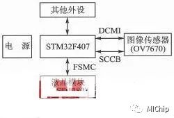
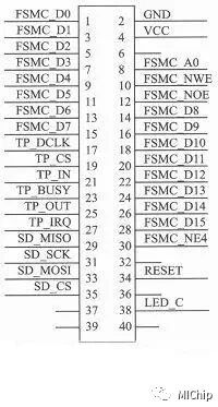
When connecting the STM32F407 to the TFT LCD module, it can be treated as an SRAM. The specific connection method is shown in Figure 2. The only thing to note is that the RS and CS pins of the LCD module are connected to the FSMC controller of the STM32F407. In this system, RS is connected to FSMC_A0 (PF0), and CS is connected to FSMC_NE4 (PG12). These connections directly relate to the register address settings during software initialization.
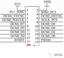
As shown in the figure, when connecting the STM32F407 to the OV7670, the OV7670’s XLCK PC9 can select either the MC01 or MC02 pins of the STM32F407. The PCI SOIC and SOID PC2 pins can be connected to the I2C bus, or other I/O pins can be defined according to the software design (this system adopts this scheme), and the other ports of the OV7670 are connected to the corresponding DCMI interface.
Software Implementation
The key points of the software design in this system are the configuration of the system clock, initialization of the TFT LCD module, initialization of the OV7670 image sensor, and simulation of SCCB bus timing. The software program flowchart is shown in the figure.

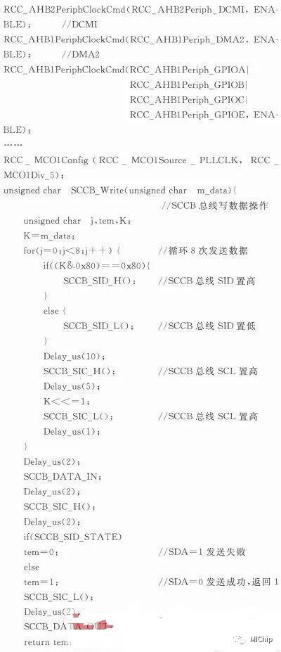
The system clock configuration is completed by the RCC_Config() function, and the internal structure of the function is as follows:

The key point of the TFT LCD module initialization is the configuration of the FSMC controller and the calculation of register addresses. The FSMC of the STM32F407 uses the clock signal provided by AHB3, so it is necessary to enable the AHB3 clock and the clock signals of other I/O ports that the FSMC controller reuses. The register addresses need to be calculated based on the specific connection method of the RS and CS pins of the LCD module to the FSMC interface. The address mapping for external devices by the FSMC controller of the STM32F4 series microprocessors starts from 0x60000000 and ends at 0x9FFFFFFF, consisting of 4 BANKs, each BANK being 256 MB in size, and each BANK is further divided into 4 blocks, each block being 64 MB in size.
In the TFT LCD initialization program, BANK1 is selected, and since CS is connected to FSMC NE4 (PG12), the starting address of the TFT LCD module’s registers is 0x6C000000; RS is connected to FSMC_A0 (PF0), so the RAM of the TFT LCD module is 0x6C000000 + 20×2 = 0x6C000002. If BANK1 is selected in the TFT LCD initialization program and CS is connected to FSMC NE1 (PD7), the starting address of the TFT LCD module’s registers is 0x60000000; RS is connected to FSMC A18 (PD13), so the RAM of the TFT LCD module is 0x60000000 + 218×2 = 0x60080000.
Following this method, the starting addresses of the registers and RAM of the LCD module can be calculated for other connection methods. The code is as follows:
#define LCD_RAM *(vu16*)((u32)0x6c000002) // Define RAM base address
#define LCD_REG *(vu16*)((u32)0x6c000000) // Define REG base address
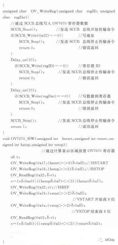
The key points for initializing the OV7670 image sensor are twofold: first, the configuration of the DCMI interface and DMA part of the microprocessor, which mainly involves enabling the clock signals for the DCMI interface, DMA controller, and other I/O ports used by the image sensor; second, the configuration of the OV7670’s own registers. Due to space limitations, some important functions are listed below with important comments for reference.
The SCCB bus timing simulation can be programmed according to the timing defined in the SCCB standard, which is well known and will not be elaborated further.
Conclusion
Conclusion
Through the programming, debugging of software and hardware, a satisfactory result has been achieved, as shown in the figure.
Although the video image display is somewhat blurry and the picture has a slight stutter, further optimization of the software and hardware can improve the image quality, while also providing ideas for the application of STM32F407 and OV7670 in video surveillance systems.
Source: Yufei Network

Disclaimer: We respect originality and emphasize sharing. The materials in this article are sourced from the internet, and the copyright belongs to the original author. If your rights are infringed, please contact the editor, and we will delete it immediately.