Title: Design and Implementation of PCIe RP System Based on Cortex-M3 Core
XU Junjie, WEI Jinghe, LIU Guozhu, HE Jian, ZHANG Zheng
(National Key Laboratory of Integrated Circuits and Microsystems)
Abstract: The Peripheral Component Interconnect Express (PCIe) and Serial Rapid IO (SRIO) are mainstream high-speed communication interface protocols. In big data application scenarios represented by artificial intelligence, achieving compatibility with these protocols is key to building high-performance computing systems and breaking through storage and computing bottlenecks. To address this need, the Chiplets Interconnect Protocol (CIP) implements multi-protocol conversion and interaction, including PCIe, SRIO, DDR, and NAND FLASH, through a unified routing network. Among these, PCIe serves as the primary human-machine interaction interface, and constructing a PCIe RP (Root Port) system is fundamental to achieving PCIe communication. Existing PCIe read/write devices based on operating systems suffer from high latency and poor operability. To solve these issues, a PCIe RP system was built based on the Cortex-M3 processor, along with corresponding driver and software development, enabling efficient and precise data transmission between PCIe and various devices. On the basis of achieving basic functionality, stability tests for large-scale data interactions of 50,000, 100,000, and 150,000 times were completed. The results indicate that the system demonstrates good stability in large-scale data interaction events, providing a solution for data exchange between the processor and PCIe.
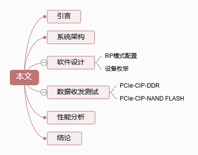 ThisArticle
 Highlights
We often regard PCIe as a “high-end” component in PCs or servers, seemingly only manageable with x86/ARM big cores + Linux. The paper by Xu Junjie et al., published in the 2025 issue 8 of the journal “Integrated Circuits and Embedded Systems”, titled “Design and Implementation of PCIe RP System Based on Cortex-M3 Core”, brings the PCIe Root Port system designed based on the Cortex-M3 core into the world of CIP (Chiplets Interconnect Protocol), using less than an A4 page of code to enable PCIe, SRIO, DDR, and NAND FLASH to handshake within the same chip network—achieving lower latency, power consumption, and development cycle compared to traditional OS solutions.
1 Why PCIe Again?
AI large models, in-vehicle intelligent driving, and industrial real-time control all rely on the dual drive of “computing power + storage”. PCIe, as the main human-machine interaction channel on the host side, is often criticized for its “heavy software stack, high latency, and poor scalability”. The traditional approach is “big core + Linux driver”, which often proves to be overkill in heterogeneous chiplet systems—resulting in losses in power consumption, startup time, and real-time performance.
2 Is Cortex-M3 Enough?
The author’s answer is: Yes! There are three reasons:
-
Real-time performance: Cortex-M3 runs bare-metal, with interrupt response in the nanosecond range, avoiding millisecond-level jitter from Linux kernel scheduling.
-
Controllable protocol stack: Based on Xilinx’s official AXI Memory-Mapped to PCIe soft core, register-level configuration completely transforms the “black box” into a “white box”.
-
Power and area efficiency: By eliminating unnecessary peripherals, a single chip can serve as a Root Port, consuming an order of magnitude less power than x86 solutions.
3 What Does the System Look Like?
In summary: M3 as the brain, AXI as the blood vessels, CIP as the highway.
-
Main control: Cortex-M3 + SWD/JTAG debug port
-
High-speed interface: AXI & AXI-Lite interfacing with PCIe soft core (configured as Root Port)
-
Interconnect network: CIP routing network translates PCIe packets into local protocols for SRIO, DDR, and NAND FLASH
-
Debugging: UART for real-time register printing, one-click download with Keil
4 Software is the Soul
The paper uses two flowcharts to clearly break down the process from “0 to successful enumeration”:
-
RP mode configuration: Write 0x1 to register 0x148 to establish Root Port identity.
-
Bar space allocation: RP 2×32 bit, EP 6×32 bit, address window configured at once for zero-copy DMA later.
-
Enumeration + MSI interrupt: Serial output “Device 0x1234 found” in real-time, making debugging very satisfying.
Data path:
-
Write to DDR: M3→PCIe→CIP→DDR, 4 Word burst, actual waveform aligns bit by bit with expected values.
-
Read from DDR: DDR→CIP→PCIe→M3, MSI interrupt triggers, Cortex-M3’s interrupt service routine directly uses memcpy, with CPU usage <5% throughout.
5 150,000 Reads and Writes, 0 Errors!
The most hardcore experimental score: The author conducted continuous read/write comparisons of 50,000, 100,000, and 150,000 times on three data channels—DDR, NAND FLASH, and SRIO—resulting in zero bit-level errors and zero link drops. The 100,000 times DDR loopback test curve presented in the paper is as stable as a straight line, completely breaking the stereotype that “small cores cannot handle big data”.
6 What Can This Bring to the Research Community?
① Chiplet interconnect prototype accelerator: For those working on AI Chiplet, storage-computing integration, or heterogeneous acceleration cards, this M3 + PCIe IP can be used as a “small baseboard” to validate routing protocols, saving the hassle of large FPGA + Linux.
② Embedded PCIe teaching template: Course design and laboratory platforms no longer need to “move servers”; a single MCU development board can allow students to fully explore enumeration, DMA, and MSI.
③ A boon for real-time control scenarios: Industrial sites and in-vehicle ECUs are sensitive to latency; the combination of M3 + PCIe is both real-time and power-efficient, and can be directly ported to ASIL-B/C level systems in the future.
This article citation format: Xu Junjie, Wei Jinghe, Liu Guozhu, et al. Design and Implementation of PCIe RP System Based on Cortex-M3 Kernel [J]. Integrated Circuits and Embedded Systems, 2025, 25(8): 74-80. XU J J, WEI J H, LIU G Z, et al. Design and implementation of PCIe RP system based on Cortex-M3 kernel [J]. Integrated Circuits and Embedded Systems, 2025, 25(8): 74-80 (in Chinese).
NextIssueIndexNumber